Introduction: Why Chipyard
The Problem
If you work in computer architecture research, there is one question you cannot avoid: How do you build a processor platform that can actually run real software?
Not just running a Hello World and calling it a day, but booting Linux, running real applications, and ideally being able to attach custom hardware modules on top. This is the prerequisite for validating any architecture research idea.
Building all of this from scratch -- a processor core, an OS port, a toolchain -- is a legitimate approach, and you will learn a lot doing it. But it takes a very long time, often measured in semesters or years. For students who are already doing research and need a verification platform quickly, that time cost is hard to justify.
This series takes a different path -- using Chipyard directly.
What Is Chipyard
Chipyard is an open-source SoC design framework from UC Berkeley, built on the Chisel hardware description language. Its positioning has been research-oriented from the start: it does not teach you how to build a processor; instead, it gives you a ready-made infrastructure so you can focus on what you actually want to study.
The framework already integrates mature processor cores such as Rocket Core (in-order 5-stage pipeline) and BOOM (out-of-order superscalar), along with on-chip buses, memory controllers, and peripheral interfaces. It comes with Verilator/VCS simulation, FPGA prototyping, and tapeout backend support. If you need to add a custom accelerator, the RoCC and AXI4 interfaces let you plug one in directly.
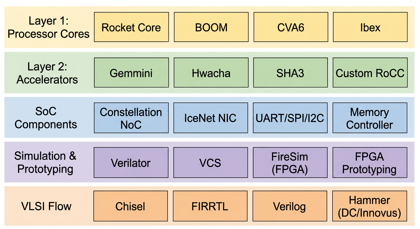
Our research group's taped-out chips heavily reuse components from Chipyard -- once the RTL design is converted to Verilog, it feeds directly into the industry-standard backend flow (VCS -> Design Compiler -> Innovus). This framework is well-established in academia, and many works published at ISCA and MICRO use it for prototype validation.
What You Can Do with Chipyard
Once you have the Chipyard environment set up, the path forward is clear.
Start by running functional simulation on a Rocket Core with Verilator to verify basic RISC-V instruction execution. After simulation is working, Rocket Core paired with a standard RISC-V Linux kernel can fully boot a Linux system -- being able to run Linux means the entire software ecosystem is available. Building on that, this series runs a custom LLM inference program on the RISC-V platform with a Gemmini systolic array accelerator, then analyzes performance bottlenecks using profiling.
From toolchain setup to running accelerated LLM inference on FPGA, the entire cycle is measured in weeks, not years.
Roadmap for This Series
- Prerequisites: Setting up the development environment -- WSL2 + proxy + VSCode
- Chapter 1: Chipyard environment setup and toolchain overview
- Chapter 2: Your first Rocket Core -- running Hello World in simulation
- Chapter 3: The tapeout perspective -- where Chipyard fits in a real chip design flow
- Chapter 4: Booting Linux on FPGA -- theory
- Chapter 5: Booting Linux on FPGA -- practice and troubleshooting
- Chapter 6: Gemmini -- hardware-accelerated matrix operations on FPGA
- Chapter 7: LLM inference with Gemmini on FPGA
Each article documents the real pitfalls encountered along the way, not just the official documentation. Basic background in digital circuits and computer architecture is assumed -- no prior knowledge of Chisel or Chipyard is required.
Next up: Prerequisites -- Development Environment Setup.
Prerequisites: Development Environment Setup -- WSL2 + VSCode
Introduction
Whether you are getting into open-source chip design or AI algorithm development, the very first hurdle is almost always setting up the environment.
Environment setup looks like "just preparation before the real work begins," but it is far from a beginner-level task. Many people get stuck here for a month or more -- not because the steps are inherently difficult, but because online tutorials are scattered and inconsistent.
This article gives you a single, field-tested setup path: WSL2 + VSCode. It works for both open-source chip development and AI work.
1. Why You Must Work on Linux
The mainstream open-source chip toolchains -- Chipyard, Verilator, OpenROAD, Yosys -- almost exclusively support Linux. The AI world is similar: CUDA toolchains and many deep-learning frameworks have far better support on Linux than on Windows.
Dual-booting Linux is an option, but switching back and forth between operating systems is painful. Running WSL1 or Cygwin on Windows solves some problems, but falls short when you need to compile complex toolchains.
WSL2 (Windows Subsystem for Linux 2) is the most practical solution available today. It lets you run a full Linux system directly inside Windows -- no dual-boot, no virtual machine. Both systems run side by side with shared file access. Under the hood it runs a real Linux kernel, not an emulation layer, so the vast majority of Linux tools work out of the box with near-native performance.
You might ask, "Why not just use Docker?" -- Once WSL2 is set up, Docker Desktop can use WSL2 as its backend. If you ever need a containerized environment later, the transition is seamless.
2. Why VSCode Remote-WSL
Working directly in the WSL2 terminal is perfectly possible, but for large projects like Chipyard the pure-terminal experience is rough -- deep directory trees, searching and jumping around with nothing but the command line, and difficulty pinpointing issues when something goes wrong.
VSCode's Remote-WSL extension solves this. Once installed, VSCode connects directly into the WSL2 environment. The file tree, code completion, and integrated terminal all live in one window, giving you an experience identical to local development. The files you edit are the Linux files inside WSL2, and the terminal runs WSL2's bash -- there is no context-switching friction.
On top of that, you can install the GitHub Copilot extension in VSCode; having AI assistance while writing scripts, editing config files, or debugging environment issues is a huge productivity boost.
3. Setup Steps
3.1 Install WSL2 and Ubuntu
Open PowerShell as Administrator and run:
wsl --install
This command automatically enables WSL2 and installs Ubuntu (the latest LTS version by default). Restart your computer after it finishes. On the first Ubuntu launch, set your username and password.
Verify that WSL2 is running correctly:
wsl --list --verbose
Confirm that the VERSION column for Ubuntu shows 2.
Type wsl in PowerShell to enter the Ubuntu environment, then update your packages:
sudo apt update && sudo apt upgrade -y
3.2 Install VSCode and the Remote-WSL Extension
On the Windows side, download and install VSCode. Once installed, open the Extensions Marketplace and search for and install Remote - WSL (the official Microsoft extension).
In the WSL2 terminal, navigate to your working directory and run:
code .
VSCode will automatically open in Remote-WSL mode. If the bottom-left corner shows "WSL: Ubuntu," the connection is successful.
Recommended extensions (install on the WSL side, all optional):
- C/C++ (IntelliSense and debugging support)
- Scala (Metals) (essential for Chisel/Scala development)
- verilog-hdl (Verilog syntax highlighting)
4. Closing Thoughts
At this point your development environment is ready. Whether you are about to clone Chipyard, install a toolchain, or work on an AI project, this setup has you covered.
One last note: environment setup is actually a core research skill, not a trivial chore. Research frequently involves reproducing open-source work, and the main obstacle to reproduction is often not understanding the paper -- it is getting the code to run. Dependency version conflicts, toolchain incompatibilities, failed downloads... these are all environment problems. Building solid environment-setup skills is a prerequisite for efficiently leveraging open-source work.
Next up: Chapter 1 -- Chipyard Environment Setup and Toolchain Configuration.
Chapter 1: Chipyard Environment Setup -- Clone, Initialize, and Toolchain Configuration
1. Introduction
Starting from this chapter, we get our hands dirty. The prerequisite is that everything from the prep chapter is already in place -- WSL2 is running and VSCode is connected to WSL2.
This chapter covers two things: first, understand how Chipyard is organized from a high level; then get the environment up and running. The operations themselves are not complicated -- mostly waiting. But if you don't know what each step is doing, the waiting becomes painful, and when something goes wrong you won't know where to look.
2. Understanding What Chipyard Is
What Chipyard Can Do
Chipyard is not just a processor -- it is a complete research infrastructure spanning from RTL design all the way to tapeout. Its core philosophy: get the common building blocks right (processor cores, buses, peripherals, toolchains) so that researchers can focus on their own innovations.
Here are some concrete examples of what you can do once you learn Chipyard:
Attach a custom matrix-multiply accelerator next to a Rocket Core (via the RoCC interface), run neural network inference with hardware-software co-design, and quantify the speedup -- this is the most common use case for researchers working on AI accelerators. Or tweak the processor's cache parameters (capacity, associativity, replacement policy), run simulations to compare performance across different configurations, and support architecture research. You can also bring up the design on an FPGA and actually boot Linux on your processor, running real software -- this is one of the core goals of this series, and later chapters will walk through it step by step. Or go all the way through the Hammer flow to the physical design backend, pushing the design from Chisel source code to GDS. Many works published at ISCA and MICRO use Chipyard as their prototyping and validation platform.
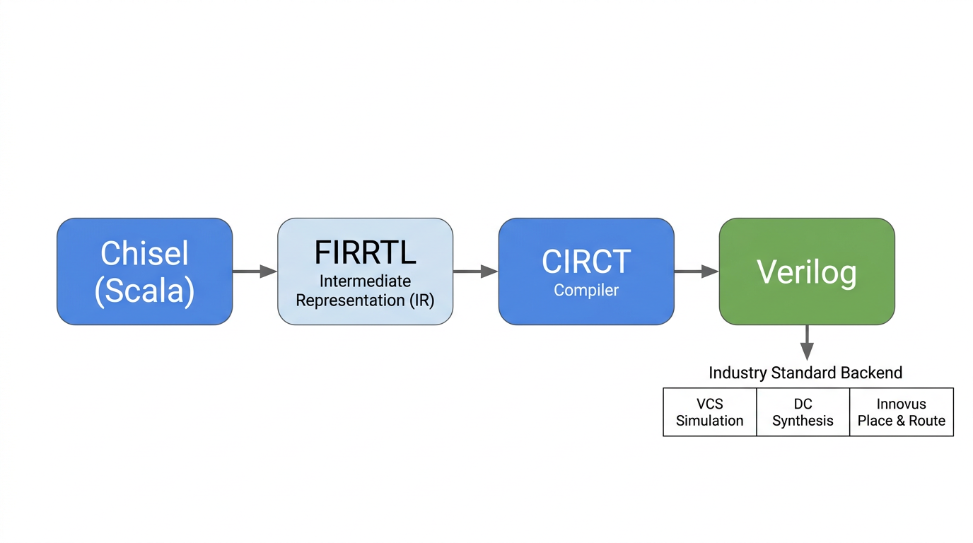
The Chisel to FIRRTL to Verilog Compilation Flow
Hardware in Chipyard is written in Chisel (a hardware description language embedded in Scala), not traditional Verilog. This is worth explaining.
Verilog describes "a specific circuit," while Chisel describes "a program that can generate circuits." Take a processor as an example: different configurations of Rocket Core (single-issue / multi-issue, different cache sizes, with or without FPU) can all be generated from the same Chisel codebase by changing parameters. In Verilog, you would need to maintain multiple near-duplicate copies of the code. This "generator mindset" is the fundamental source of Chipyard's flexibility.
The compilation flow is: Chisel source code -> FIRRTL (a hardware intermediate representation, analogous to IR in a software compiler) -> standard Verilog, produced by the CIRCT toolchain. Once you have Verilog, you can plug into any industry-standard backend tool flow (VCS simulation, Design Compiler synthesis, Innovus place-and-route) -- there is no difference from a design written directly in Verilog.
This series will not dive deep into Chisel syntax, but if you want to learn it systematically, the recommended resource is UCB's official Chisel Bootcamp -- Jupyter Notebook format, runnable online.
Main Directory Structure
After cloning, take a quick look at the directory layout -- it will help with everything that follows:
| Directory | Purpose |
|---|---|
generators/ | Chisel source code for processor cores and accelerators (Rocket, BOOM, Gemmini, etc.) |
sims/ | Simulation entry point -- this is where you run simulations (verilator/ and vcs/ subdirectories) |
toolchains/ | RISC-V cross-compilation toolchain |
software/ | Software that runs on the processor (bare-metal test programs, Linux workloads, etc.) |
vlsi/ | Tapeout backend (Hammer flow) |
fpga/ | FPGA prototyping |
env.sh | Script you must source every time you enter the working environment |
3. Cloning Chipyard
It is recommended to clone into your WSL2 home directory. Do not place it under /mnt/. The reason is that /mnt/ mounts the Windows filesystem, whose IO performance is much slower than the native Linux filesystem -- the difference becomes very noticeable when building large projects.
git clone https://github.com/ucb-bar/chipyard.git
cd chipyard
4. Initialization: What build-setup.sh Does
Run the initialization script:
./build-setup.sh
This script performs the following steps in order:
Step 1: Set up the Conda environment. Chipyard has very precise version requirements -- specific versions of Java, Scala, Python packages. If versions are wrong, the build will fail outright. Conda (a cross-platform package manager) locks down all dependency versions in an isolated environment, completely separate from the system. This is why we don't just apt install things: apt installs the latest system version, which is very likely to mismatch what Chipyard requires.
Step 2: Initialize submodules. Chipyard is a large monorepo. Rocket Chip, BOOM, Gemmini, and others are each independent Git subrepositories. This step clones them all -- there are many and they are large, so it takes a while.
Step 3: Build the RISC-V toolchain. This builds riscv64-unknown-elf-gcc (the RISC-V cross-compiler, used to compile C programs into binaries that run on a RISC-V processor) and other tools from source. This is the most time-consuming step of the entire initialization -- it involves compiling GCC from source, which can take 30 minutes to an hour depending on your machine.
Step 4: Pre-compile Scala sources. The first Chisel/SBT build is very slow (SBT is the Scala build tool). Pre-compiling saves time on every subsequent launch.
Step 5: Install CIRCT. The compiler backend for Chisel, responsible for converting FIRRTL into standard Verilog.
The whole process takes 1--3 hours, depending on network speed and machine performance. Just wait.
5. Activating the Environment
After initialization is complete, every time you open a new terminal to work with Chipyard, you need to run:
source env.sh
This command does two things: activates the Conda environment and adds the RISC-V toolchain path to PATH. After running it, the terminal prompt will show the Conda environment name (something like (.conda-env)), indicating successful activation.
If you forget to source, subsequent build and simulation commands will report "tool not found" errors -- this is the most common issue. If you hit it, check this step first.
6. Verifying the Toolchain
After source env.sh, check that the key tools are working:
riscv64-unknown-elf-gcc --version   # RISC-V cross-compilation toolchain
spike --help 2>&1 | head -1         # ISA-level simulator, first line shows version info
verilator --version                 # RTL simulator
If all three commands produce version information, the environment is ready. As a reference, my environment shows GCC 13.2.0, Spike 1.1.1-dev, and Verilator 5.022. Your exact versions may differ -- as long as you get output, you are good to go.
7. Wrapping Up
At this point, the Chipyard environment is set up and the toolchain is sorted out. There are not many pitfalls in the process -- it is mostly about waiting and understanding what each step does.
Next up: Chapter 2: Your First Rocket Core -- Running a Hello World Simulation, where we dive into the actual hardware simulation workflow.
Chapter 2: Your First Rocket Core -- Running Hello World in Simulation
1. Introduction
Last chapter we got the environment set up and verified the toolchain. This time we're doing something pretty cool: running a real RISC-V application on a processor that's simulated entirely in software.
Building a processor from scratch and getting your first program to run on it is typically a semester-long journey. With Chipyard, you can do it today. You'll see "Hello world from core 0, a rocket" printed in your terminal -- output from a full RISC-V processor core, all running on your own machine.
The simulator we'll use is Verilator -- open-source and free. Anyone can follow along; no commercial EDA license required.
2. The Complete Simulation Flow
Let's start with a fundamental question: what does it mean to simulate a processor in software?
We don't have a physical RISC-V chip on hand, but we can use software to precisely model its behavior -- every clock cycle, every signal transition, all executed according to the hardware description language specification. This is RTL simulation (Register Transfer Level simulation). Its results are fully equivalent to real silicon. It's the standard method for verifying hardware design correctness and a critical step every chip must go through before tape-out.
The simulation flow in Chipyard looks like this:
Chisel source code (under generators/ directory)
    ↓ SBT build + CIRCT
Verilog (under sims/verilator/generated-src/ directory)
    ↓ Verilator compilation
C++ executable simulator
    ↓ Run
Simulation output (terminal prints / waveform files)
Verilator converts Verilog into equivalent C++ code, then compiles it into a native executable. This is much faster than traditional event-driven simulators (like ModelSim) and is well-suited for running complete software programs.
If you want to see what the generated Verilog looks like, after running make you can browse the sims/verilator/generated-src/chipyard.harness.TestHarness.RocketConfig/gen-collateral/ directory. It contains .sv files for every module -- things like AMOALU.sv, ICache.sv -- all auto-generated from Chisel, fundamentally no different from hand-written Verilog.
3. Rocket Core Architecture
Before running the simulation, let's understand what we're actually simulating.
Rocket Core is an open-source in-order 5-stage pipeline RISC-V processor core from UCB, implementing the RV64GC instruction set (64-bit integer, multiply/divide, floating-point, and compressed instructions). An in-order 5-stage pipeline means instructions execute sequentially with no out-of-order issue -- a relatively simple structure that makes a good baseline configuration for research.
Its Chisel source code lives under generators/rocket-chip/src/main/scala/rocket/. Key files:
| File | Contents |
|---|---|
Core.scala | Pipeline top level, wiring all stages together |
Frontend.scala | Fetch frontend, includes branch prediction |
ICache.scala | Instruction cache |
DCache.scala | Data cache |
ALU.scala | Arithmetic logic unit |
CSR.scala | Control and status registers (privilege levels, interrupts, etc.) |
The Rocket Core pipeline structure is shown below -- Fetch, Decode, Execute, Memory, and Commit stages. If you've taken a computer architecture course, this should look familiar. In the diagram, PCGen is the address generation portion of the Fetch stage and isn't counted as a separate stage. Attached alongside are the FPU, Mul-Div unit, and the RoCC (Rocket Custom Co-processor) interface for connecting custom accelerators:
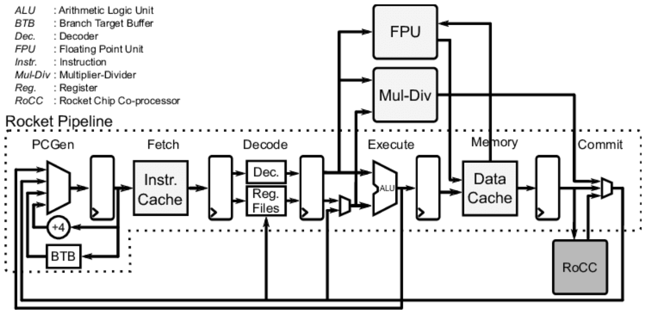
The RoCC interface in the lower-right corner of the diagram is the key entry point for attaching custom accelerators later on. If you're curious, you can open Core.scala and use this diagram to understand how all the modules are connected.
4. RocketConfig: Building-Block SoC Configuration
Chipyard uses Configs to describe the composition of an entire SoC. Different Configs correspond to different hardware configurations. The definition of RocketConfig is in generators/chipyard/src/main/scala/config/RocketConfigs.scala. Let's take a look:
class RocketConfig extends Config(
  new freechips.rocketchip.rocket.WithNHugeCores(1) ++  // One Rocket Core
  new chipyard.config.AbstractConfig)                   // Base SoC peripherals (bus, memory, UART, etc.)
Just two lines -- stack a Rocket Core on top of the base SoC configuration. The same file contains other Configs you can compare:
class DualRocketConfig extends Config(
  new freechips.rocketchip.rocket.WithNHugeCores(2) ++  // Two cores instead
  new chipyard.config.AbstractConfig)

class TinyRocketConfig extends Config(
  new freechips.rocketchip.rocket.With1TinyCore ++       // Small core: no L2$, reduced pipeline
  new chipyard.config.AbstractConfig)
This is the core design philosophy of Chipyard Configs -- compose different With* modules using ++, assembling your SoC like building blocks without modifying any hardware source code. When we add a custom accelerator later, it's the same approach: just append one more line to the Config.
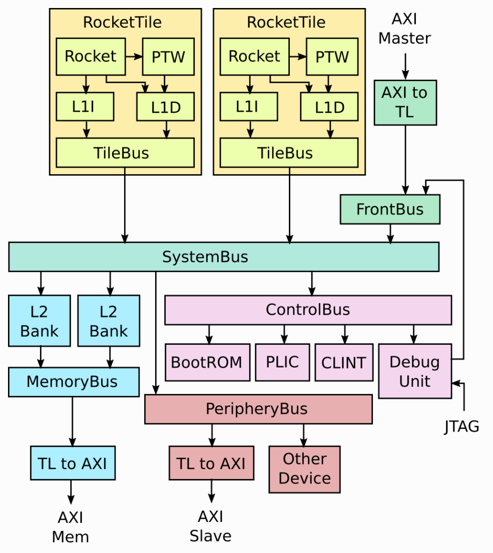
Rocket Core doesn't exist in isolation. It's wrapped inside a RocketTile, which contains the core itself, L1 instruction cache (L1I), L1 data cache (L1D), and page table walker (PTW). The RocketTile connects to the L2 cache, memory controller, and various peripherals through the SystemBus. That's why RocketConfig only needs a single WithNHugeCores(1) line -- the bus, L2, and peripherals are all already defined in AbstractConfig. The complete SoC structure is shown below:
5. Compiling the Test Program
The Hello World source code is in tests/hello.c. It's straightforward:
#include <stdio.h>
#include <riscv-pk/encoding.h>
#include "marchid.h"
#include <stdint.h>

int main(void) {
  uint64_t marchid = read_csr(marchid);   // Read the marchid CSR register
  const char* march = get_march(marchid); // Look up the processor name
  printf("Hello world from core 0, a %s\n", march);
  return 0;
}
The only difference from a typical Hello World is the extra step of reading the marchid CSR -- this way the output string changes with the processor configuration rather than being hardcoded. It's worth noting that in theory, you can write any C program, cross-compile it the same way, and run it on this processor -- that's what "a complete software execution environment" means. We're using the RISC-V cross-compilation toolchain here; you can't use a regular gcc -- a regular gcc produces x86 binaries that won't run on a RISC-V processor. riscv64-unknown-elf-gcc specifically compiles C code into RISC-V instruction set binaries.
source env.sh
cd tests
cmake -S ./ -B ./build/ -D CMAKE_BUILD_TYPE=Debug \
  -D CMAKE_C_COMPILER=riscv64-unknown-elf-gcc \
  -D CMAKE_CXX_COMPILER=riscv64-unknown-elf-g++
cmake --build ./build/ --target hello
The build artifact is tests/build/hello.riscv, a RISC-V ELF executable. The program is linked to address 0x80000000 (Rocket Core's DRAM base address). The simulator loads it to this address and has the processor begin execution from there.
6. Building the Simulator
cd sims/verilator
make CONFIG=RocketConfig
This command first triggers the SBT build (Chisel to Verilog), then invokes Verilator to compile it into an executable simulator. The first run takes a while; subsequent runs skip recompilation if the hardware code hasn't changed.
The output artifact is sims/verilator/simulator-chipyard.harness-RocketConfig.
7. Running the Simulation
cd sims/verilator
./simulator-chipyard.harness-RocketConfig \
  ../../tests/build/hello.riscv
Output:

"Hello world from core 0, a rocket" -- simulation successful.
As we saw in the source code earlier, a rocket comes from looking up the marchid CSR value, not from a hardcoded string. If you run this with a BOOM Config instead, it would print "boom".
8. Optional: Generating Waveforms
Adding the debug target builds a simulator with waveform output enabled:
make CONFIG=RocketConfig debug
mkdir -p output
./simulator-chipyard.harness-RocketConfig-debug \
  +permissive \
  +vcdfile=output/hello.vcd \
  +permissive-off \
  ../../tests/build/hello.riscv
The waveform file is at sims/verilator/output/hello.vcd. I recommend opening it with Surfer (there's also a VSCode plugin -- just search for Surfer and install it). The Scopes panel on the left lets you browse the entire SoC hierarchy. Select the signals you're interested in, and the right panel will show their values at each clock cycle:
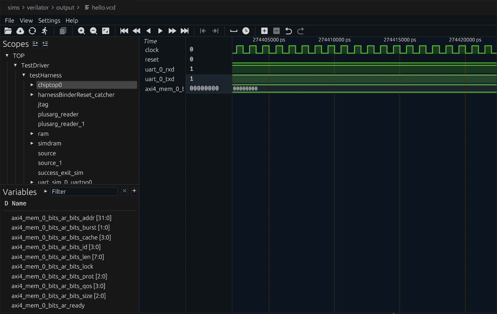
Waveforms are the most direct tool for debugging custom hardware. Once you've added a custom accelerator, waveforms let you see exactly how signals change on every clock cycle, making it fast to pinpoint issues.
9. Wrapping Up
The first Rocket Core simulation is up and running. Let's recap what we did: we compiled a RISC-V program with the cross-compilation toolchain, used Verilator to compile a Chisel design into a simulator, then had the processor execute the program and saw its output. The entire flow from source code to result, all completed locally.
This chapter covered a lot of ground, and it can feel overwhelming if you're new to this. But here's the good news: this is already the complete workflow at the software level. Going forward, whether you're switching to a more complex processor configuration, adding a custom accelerator, or running larger programs, you'll be optimizing or swapping out individual steps within this framework -- not building a new flow from scratch. Once you understand this pipeline, everything else is filling in details.
Next up: Chapter 3: The Tape-Out Perspective -- Where Chipyard Fits in a Real Chip Design Flow, stepping back from simulation to see how Chipyard designs connect to the industry tape-out backend.
Chapter 3: The Tapeout Perspective -- Where Chipyard Fits in a Real Chip Design Flow
In the first two chapters, we stayed entirely at the simulation level -- compiling RISC-V programs and running them on a software-modeled processor built with Verilator. But for those of us doing chip research, simulation is just a means to an end. The ultimate goal is to tapeout the design and verify it on real silicon.
This chapter is not a step-by-step how-to. Instead, it draws a "map": where Chipyard sits in the overall chip design flow, what portion of the flow it owns, how its outputs connect to industry-standard backend tools, and what kinds of engineering constraints you typically run into during an academic tapeout.
1. The Full Path from Design to Tapeout
A digital chip goes through roughly the following stages from design to final tapeout:
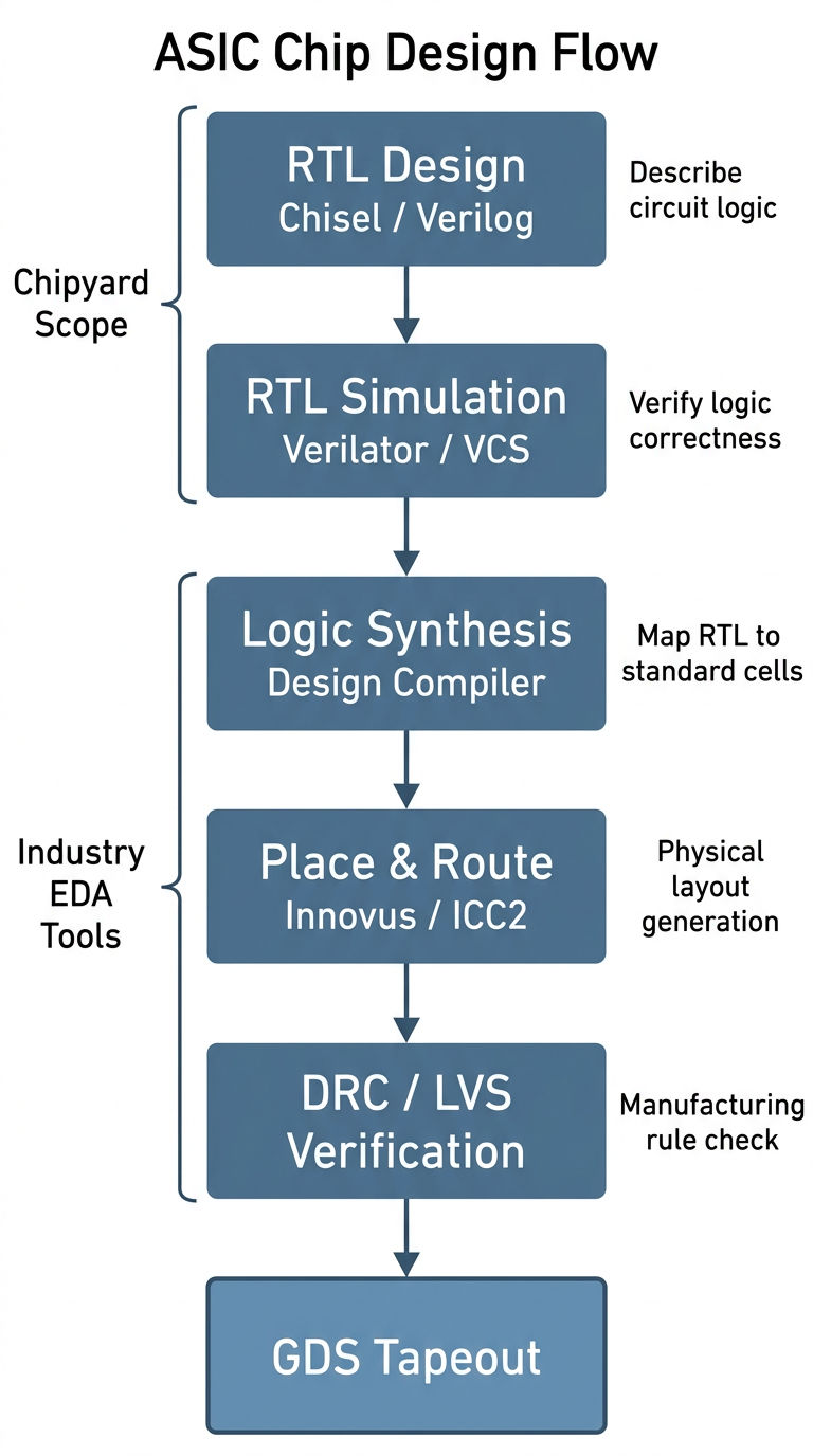
Let's walk through what each stage does.
RTL design is the starting point of the entire flow. RTL (Register Transfer Level) is an abstraction layer that describes the logical behavior of digital circuits -- when you write in Verilog or Chisel that "this module takes these inputs, produces these outputs, and its internal registers change in this way," you are doing RTL design. This step captures the logic of the circuit without touching physical implementation.
RTL simulation and verification confirms at the software level that the logic design is correct. Before tapeout, you must thoroughly verify that the RTL behaves as expected. What we did with Verilator in the previous two chapters is exactly this step; in industry, VCS is the more common tool.
Synthesis is the first major "leap" in the flow -- it translates the abstract RTL description into a netlist composed of real standard cells (AND gates, OR gates, flip-flops, and other basic logic elements). This step is performed by tools like Design Compiler (DC) and requires a process technology library, because different technology nodes have different standard cells. The result of synthesis is a list of "which gates to use and how to connect them," but at this point there is no physical placement information.
Place and route transforms the synthesized netlist into an actual chip layout: first, all standard cells are placed onto the chip area (placement), then metal wires connect them together (routing). This step is performed by tools like Innovus or ICC2, and the output is a layout with precise physical coordinates and routing.
DRC / LVS verification is the final gate before tapeout. DRC (Design Rule Check) confirms that all line widths, spacings, via dimensions, and other parameters in the layout meet the foundry's manufacturing requirements. LVS (Layout vs. Schematic) confirms that the physical layout's connectivity matches the synthesized netlist exactly. Both must pass before you can submit the GDS file for tapeout.
GDS (GDSII format) is the final file format for the chip layout. It contains graphical data for all layers; the foundry uses it to fabricate photomasks and begin the lithography process.
The entire pipeline can be understood in two halves: the first two steps (RTL design + simulation/verification) focus on logical correctness and are the main battlefield for a designer's creative work; the later steps (synthesis, place and route, verification) focus on physical realizability and rely more on tools and engineering experience. Chipyard is responsible for the first half.
For researchers working in digital design, innovations are mostly concentrated at the RTL level -- new processor microarchitectures, accelerator designs, interconnect structures, etc. -- and are ultimately expressed as RTL. Of course, there is another class of research where the innovation lies in designing a custom hard macro, such as a compute-in-memory array or an analog circuit block, and RTL is just the wrapper that instantiates it. In either case, the steps after synthesis are largely engineering execution problems, driven by tools and experienced engineers. Chipyard's value is in making the path from "digital design to tapeout-ready RTL" smooth enough that researchers can focus their energy on real innovation rather than on building infrastructure.
2. Why Chipyard's RTL Can Plug Directly into an Industrial Backend
You might wonder: Chisel is a relatively new hardware description language -- do industrial EDA tools even recognize it?
The answer is: industrial tools don't need to recognize Chisel, because the final output of Chisel compilation is standard Verilog. This means that as long as the generated Verilog is correct, the downstream synthesis and place and route flow is identical to hand-written Verilog from the tools' perspective. DC and Innovus see an ordinary Verilog design; they don't know, and don't need to know, how that Verilog was generated.
Chipyard also handles another important detail: special structures like SRAMs, clock gating cells (ICGs), and IO pads correspond to different physical macros under different process technologies and cannot be described with generic RTL. When generating Verilog, Chipyard automatically turns these structures into blackboxes -- only the interface is preserved, with an empty interior. During synthesis, the backend engineer simply replaces each blackbox with the real macro from the target technology. This design allows Chipyard-generated RTL to adapt to different technology nodes without modifying any source code.
3. Chipyard's Role in a Real Tapeout: A First-Hand Example
Let me walk through an academic tapeout I participated in to show how Chipyard is actually used in practice.
Step 1: Write a Config for ASIC requirements and export Verilog.
Resources in academic tapeout are extremely limited, and pad count is a key constraint. The more chip pins you have, the larger the pad ring, and the higher the cost. The default Chipyard configuration includes an AXI4 DDR interface, which requires hundreds of pins -- prohibitively expensive for tapeout.
Chipyard's Config mechanism proves its worth here: by modifying Config parameters -- without touching any RTL source code -- you can replace the external memory interface with SerialTL, an extremely compact serial interface with only a handful of signal lines. This change is done entirely at the Scala configuration level; not a single line of the underlying Rocket Core, bus, or cache RTL is modified.
Once the Config is ready, a single command generates synthesis-ready Verilog with SRAM blackboxes and IO pad placeholders, along with the corresponding simulation file package.
Step 2: Pre-synthesis simulation with VCS.
After exporting Verilog, run pre-synthesis simulation on VCS first to confirm functional correctness. The previous two chapters used Verilator; when interfacing with a tapeout flow, you typically switch to VCS -- it is the industry-standard simulator, is more consistent with the downstream synthesis environment, and makes it easier to debug discrepancies between simulation and synthesis results.
Step 3: Replace blackboxes and run DC synthesis.
Replace the SRAM blackboxes and ICG placeholders in the Verilog with macros from the foundry-provided technology library, add behavioral models for IO pads and analog blocks, apply constraint scripts, and hand everything to Design Compiler for synthesis. From this step onward, Chipyard's job is done -- the flow is entirely standard industrial ASIC digital backend.
A note on Hammer: Chipyard includes the Hammer framework, which aims to automate the backend steps described above. In practice, however, industrial EDA tools have varying invocation interfaces and complex license management, and Hammer's adaptation scripts require careful tuning for specific tool versions. For teams that already have a mature set of backend scripts, reusing the existing flow is often the better choice -- Chipyard just delivers clean Verilog, and the backend stays untouched. Hammer is better suited for scenarios where you are building a backend flow from scratch.
4. A Typical Challenge in Academic Tapeout: No Access to Analog IP
Commercial chips use a large amount of analog IP: DDR PHYs, SerDes, PLLs, IO drivers, and so on. These IPs typically require licensing agreements with the foundry or IP vendor, which academic tapeouts often cannot obtain.
The solution is FPGA bridging: the chip side retains only a simple digital interface, and an FPGA handles the DDR controller, external memory, and even test stimulus generation. The chip interacts with the FPGA through this digital interface, effectively offloading analog IO functions.
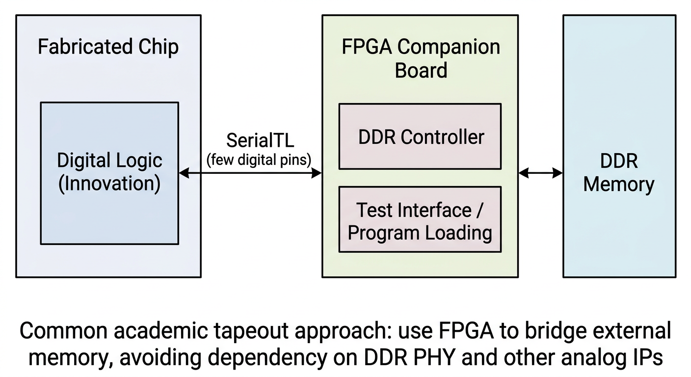
This is exactly the typical use case for the SerialTL interface. Chipyard's SerialTL can be thought of as a "host protocol": the FPGA runs a TSI server that handles memory reads/writes and program loading; the chip side sends requests over SerialTL, accessing DDR on the FPGA side as if it were local memory. The entire scheme is already implemented in Chipyard's FPGA support -- no additional development is needed.
Post-tapeout testing is considerably more complex, but that is beyond the scope of this series for now. If the opportunity arises, I may write a dedicated tapeout column to cover it in detail.
5. Summary
Chipyard's position in the overall chip design pipeline should now be fairly clear: it handles the front end -- RTL generation and simulation/verification -- and outputs standard Verilog that plugs seamlessly into an industrial backend. Through the blackbox mechanism, it provides clean replacement interfaces for SRAMs, ICGs, and IO pads. Through the Config mechanism, it lets you tailor interfaces and adjust parameters without ever touching RTL source code.
With this "map" in mind, you can see where every task you perform fits within the full tapeout pipeline -- whether you are tweaking a Config parameter or running a simulation, the purpose behind it becomes much clearer.
Next up: Chapter 4 -- Booting Linux on an FPGA: A Chipyard Field Report. We will get Linux actually running -- not just inside a simulator, but on an FPGA.
Chapter 4: Booting Linux on an FPGA -- A Field Guide (Theory)
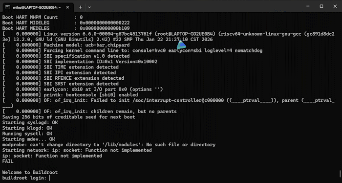
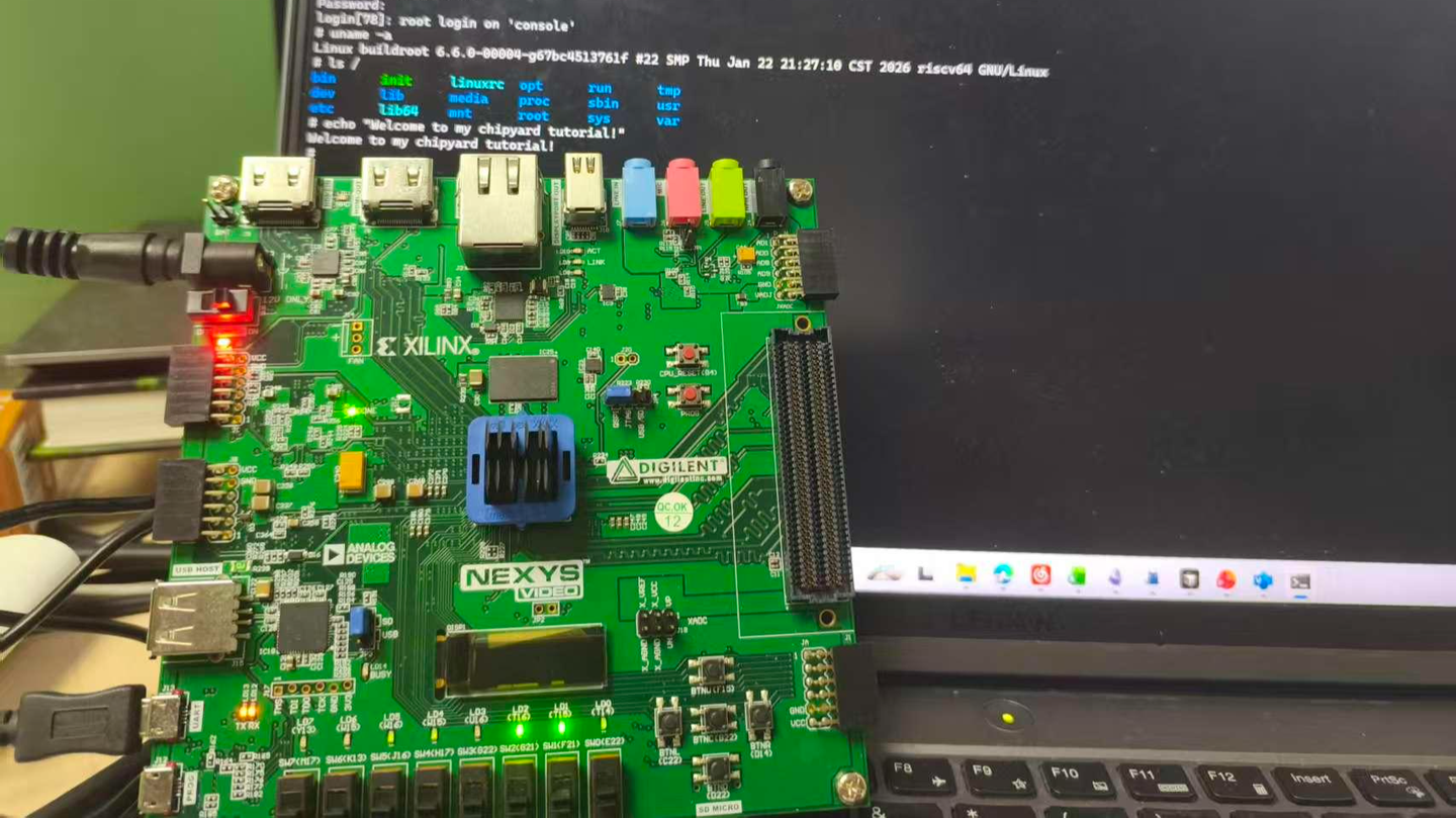
An FPGA development board running a Rocket Core generated by Chipyard -- the same processor we simulated in the previous chapters -- displaying a Linux login prompt and accepting commands.
In the earlier chapters we stayed entirely within the simulation layer. Starting from this chapter, the goal levels up: get Linux running on a real FPGA board.
Before we get our hands dirty, though, let's first understand how Linux actually boots. Without that knowledge, when something breaks you won't know which layer to blame, which log to check, or why a particular configuration is necessary. This chapter covers the theory; the next one covers the hands-on practice.
1. The Big Picture: Two Independent Tasks
Running Linux on an FPGA is essentially two independent tasks.
Hardware side: Use Vivado to synthesize the Verilog generated by Chipyard into a bitstream and program it into the FPGA. An FPGA is fundamentally a programmable logic device -- a blank canvas out of the box. The bitstream is the circuit configuration written onto that canvas. Once programmed, the FPGA becomes a real RISC-V processor board running a Rocket Core, with real DDR memory, a real clock, and real I/O.
Software side: Build the software stack (OpenSBI + Linux kernel + root filesystem) on the host machine, package it into an ELF file, and transfer it to the FPGA's DDR over a UART serial link. ELF is an executable file format that contains the program's machine code along with load-address information; the host-side tool writes each segment into the correct DDR location.
The two tasks are independent and can be debugged separately -- once the bitstream is programmed, you don't need to touch it again. If the software has a problem, just fix it and reload; no re-synthesis required. This is a very practical aspect of Chipyard's prototyping workflow: synthesizing a bitstream typically takes tens of minutes, whereas reloading software takes only a few minutes.
2. The Software Stack: Four Layers
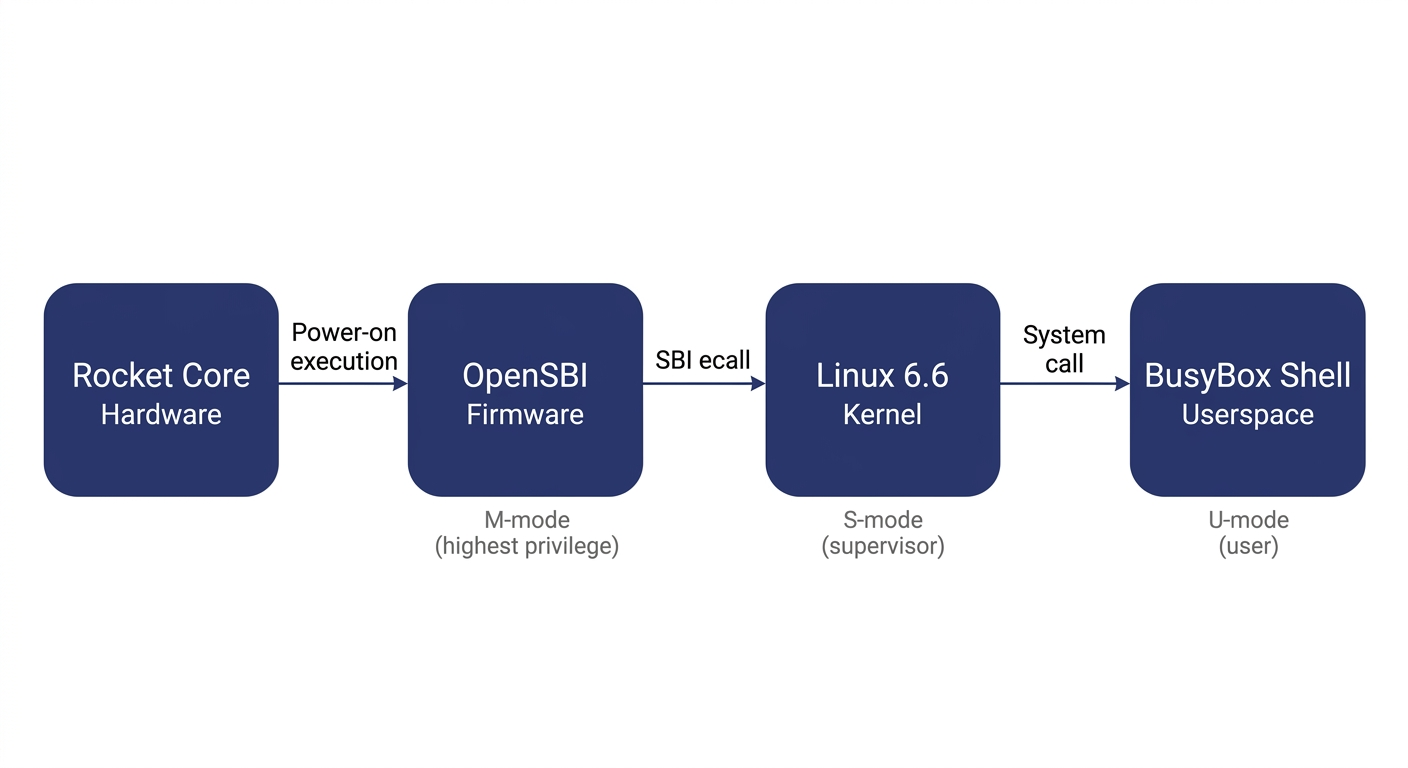
Booting Linux on RISC-V involves four layers:
Before explaining each layer, let's clarify the concept of privilege levels -- it is the key to understanding the entire stack.
Modern processors implement a privilege hierarchy to provide isolation and protection. Software running at a lower privilege level cannot freely access hardware registers or read/write another program's memory -- any attempt to do so triggers a processor exception. RISC-V defines three privilege levels: M-mode (Machine mode, the highest privilege, with access to everything), S-mode (Supervisor mode, mid-level privilege, where the operating system runs), and U-mode (User mode, the lowest privilege, where ordinary applications run). Each software layer can only invoke services from the layer below it through well-defined interfaces; it cannot bypass layers and manipulate hardware directly.
OpenSBI runs in M-mode. It is the most privileged software layer in the entire system and the very first code to execute after power-on. It has two responsibilities: first, it performs the lowest-level hardware initialization (e.g., configuring the interrupt controller and setting up memory protection); second, it exposes the SBI (Supervisor Binary Interface) to the layer above (Linux) -- a standardized set of service calls that Linux can invoke via the ecall instruction, such as printing a character, setting a timer, or bringing a core online. SBI is analogous to the abstraction layer that BIOS/UEFI provides to the OS in the x86 world. It is worth noting that OpenSBI is not the only way to boot Linux on RISC-V -- other SBI implementations like RustSBI exist, and there are also SBI-independent boot paths such as LinuxBoot and UEFI. We use OpenSBI here because Chipyard integrates it by default, making it ready to use out of the box.
The Linux kernel runs in S-mode and is the operating system we all know. In theory, Linux could drive UART hardware directly through a standard UART driver. However, in our configuration the UART hardware is occupied by the UART-TSI protocol (used for program loading and HTIF communication) and is not exposed to Linux. Therefore, the Linux console must go through the SBI-provided console interface, and the driver must be configured as hvc0 (the SBI virtual console) rather than the usual ttyS0 (which talks directly to UART hardware). This is a common pitfall for first-time users, and the hands-on chapter will address it in detail.
The root filesystem is the filesystem Linux mounts after booting. It contains the shell, basic commands (ls, cat, etc.), and library files. We use Buildroot to construct it -- Buildroot is an embedded Linux build framework that can cross-compile a complete, minimal rootfs. The resulting root filesystem is packaged as an initramfs (a compressed filesystem embedded inside the kernel image). At boot, Linux decompresses it into memory, runs /init, and ultimately drops into a BusyBox shell. BusyBox is a tool that bundles hundreds of common utilities -- ls, cat, sh, and more -- into a single executable, purpose-built for embedded scenarios with an extremely small footprint.
What actually gets loaded is a file called fw_payload.elf -- during OpenSBI's build, the Linux kernel is embedded directly inside it. The host only needs to transfer this single file. The processor starts executing at the OpenSBI entry point, and after initialization, OpenSBI automatically jumps to the kernel.
3. The Boot Process: How the Processor Wakes Up
Now that we understand the structure of the software stack, let's trace how the entire boot process is triggered.
After the FPGA is powered on and the bitstream is programmed via JTAG, the Rocket Core does not immediately run our program. Instead, it begins executing from the on-chip Boot ROM. The Boot ROM resides at address 0x1000_0000 and contains just a few dozen lines of assembly: it reads the current hart ID (the processor core number), loads the address of the DTB (Device Tree Blob -- a data structure describing what hardware is on the board and at what addresses) into a register, and then executes the WFI (Wait For Interrupt) instruction. WFI puts the processor into a low-power wait state -- literally "wait for interrupt." The processor sits there doing nothing until an interrupt arrives.
At this point the host takes over: the tool program opens the UART serial port, parses fw_payload.elf, and writes each loadable segment block-by-block into the FPGA's DDR at the specified addresses (via the UART-TSI protocol, which essentially lets the host remotely read and write the FPGA's memory). Once the transfer is complete, the tool writes a 1 to the MSIP register of the CLINT (Core Local Interruptor, the on-chip interrupt controller), triggering a software interrupt.
The Rocket Core detects the interrupt, wakes from WFI, and jumps to the DDR base address 0x8000_0000 -- the OpenSBI entry point. OpenSBI initializes the M-mode environment, sets up interrupt delegation (handing most exceptions and interrupts off to S-mode for handling), and then switches to S-mode via the mret instruction, jumping to the kernel entry point at 0x8020_0000. Linux takes over, initializes memory management and various drivers, decompresses the initramfs, runs init, and finally prints the login prompt on the terminal.
There is an elegant design choice in this process: after power-on, the processor voluntarily pauses and waits, letting the host decide when to load a program, what program to load, and where execution should begin. This is the standard mode for FPGA prototyping -- you can swap in a different program at any time without re-programming the bitstream; just press CPU_RESET and it restarts.
4. How the Console Output Reaches Your Screen
There is one more piece of the puzzle to understand: how does a character output by printf inside Linux end up appearing on your host terminal?
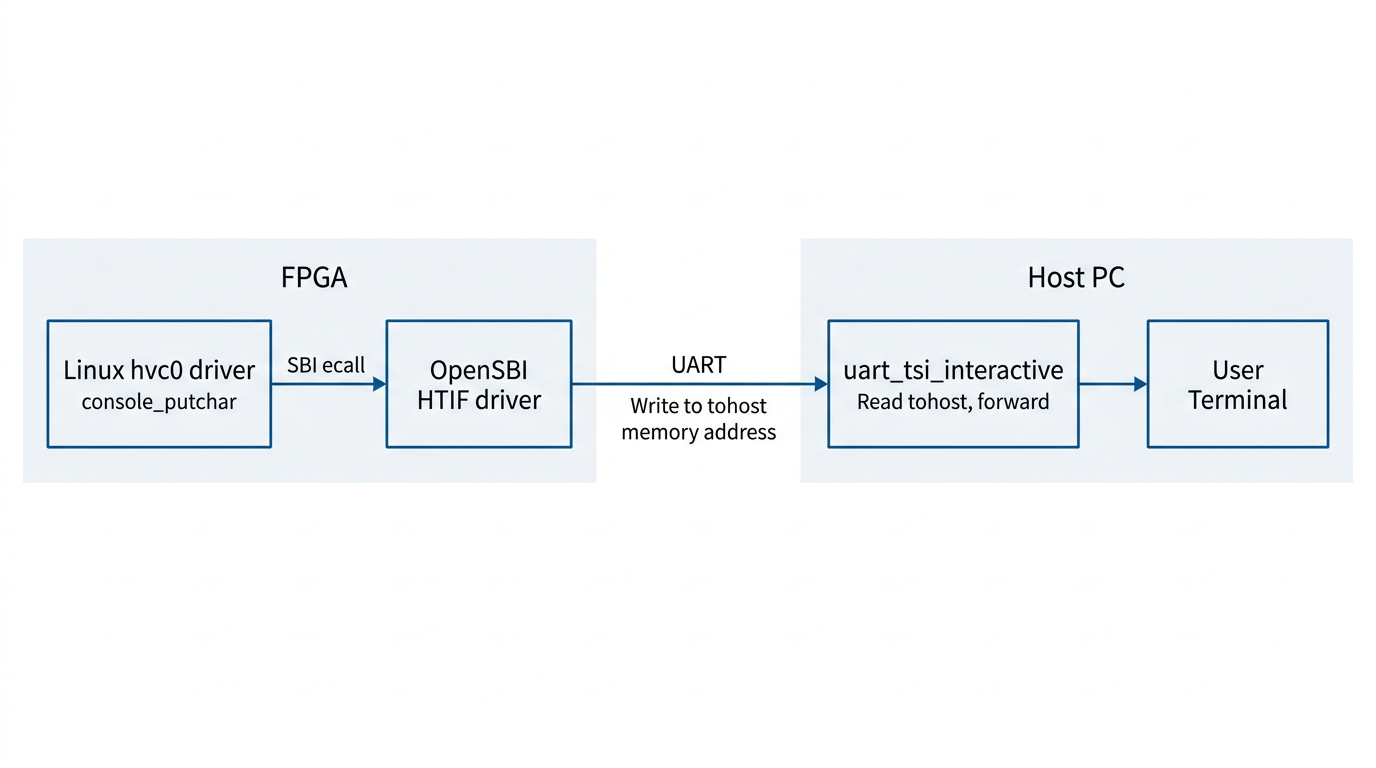
Between the processor on the FPGA and the host, there is only a single UART wire. But UART is a very simple serial protocol -- it can only carry a byte stream, with no addressing and no commands. To allow the host to both read/write the FPGA's memory (for program loading) and relay console I/O, Chipyard runs a protocol called TSI (Tethered Serial Interface) over this wire. The host sends TSI commands like "write value Y to address X," and the hardware on the FPGA side parses the command and performs the corresponding memory operation.
Console output, however, uses a different mechanism: HTIF (Host-Target Interface). When Linux outputs a character, it travels through the hvc0 driver -> SBI ecall -> OpenSBI. OpenSBI then writes the character to a specific memory-mapped address called tohost. The host-side tool continuously polls this address; when it reads data, it prints it to the terminal. In the reverse direction, when the user presses a key on the host, the tool writes the character to the fromhost address. OpenSBI reads it and returns it to Linux via SBI getchar.
The entire console I/O path operates purely through memory -- it does not depend on any additional hardware peripherals. This is also why the host-side tool must remain running for the entire duration of program execution -- it serves as the relay hub for the entire I/O path. If it exits, you lose all visibility.
5. Summary
Stringing these layers together, the logic of the entire boot process becomes clear:
FPGA power-on -> Program bitstream via JTAG -> Boot ROM WFI wait -> Host writes fw_payload.elf via TSI -> Software interrupt wakes the processor -> OpenSBI (M-mode) initializes -> Linux (S-mode) boots -> BusyBox Shell (U-mode) ready -> Console I/O relayed between memory and host via HTIF.
When something goes wrong, this chain serves as your troubleshooting map: no output at all? Check whether the host tool and TSI communication are working. Output appears but no interaction? Check whether the Linux console is configured to point to hvc0. Boot hangs midway? Check the kernel watchdog settings.
Next up: Chapter 5 -- Booting Linux on an FPGA: A Field Guide (Practice), where we roll up our sleeves, walk through each layer end to end, and document every pitfall along the way.
Chapter 5: Booting Linux on an FPGA — A Practical Troubleshooting Guide
The previous article walked through every layer of the boot flow: Boot ROM WFI wait, UART-TSI loading, OpenSBI M-mode initialization, Linux S-mode startup, and HTIF console IO forwarding. This article gets hands-on and brings the entire chain to life on real hardware.
What you'll find here is a correct, directly reproducible procedure — the steps are laid out first, and the pitfalls along with their root causes are collected in a dedicated section at the end for reference when something goes wrong.
Board used in this article: Digilent Nexys Video (Artix-7 XC7A200T).
Other FPGAs can reproduce this as well. The recommended specifications are roughly Artix-7 200T-class logic resources, external DDR, and a USB-UART interface — though the resources are not fully utilized, so smaller boards may work depending on how aggressively you trim the Config. The software-side modifications are fully portable; on the hardware side, you need to write a new Chipyard Config — see the adaptation notes at the end of this article for details.
As discussed in the theory article, running Linux on an FPGA consists of two independent tasks: on the hardware side, synthesize the Verilog into a Bitstream and program it into the FPGA; on the software side, build fw_payload.elf and transfer it into DDR to run. This article walks through both tasks in that order. The operating environment is split into two parts: synthesis and programming are done in Vivado on Windows, while software building and loading are done under WSL2. The Nexys Video has two USB ports — the PROG port connects to Vivado and the UART port connects to WSL2, so there is no conflict.
1. Building the Linux Image
If you are using the precompiled
fw_payload.elffrom the companion repo, skip Sections 1 and 2 and go directly to Section 3.
The Nexys Video has only one UART, and it is occupied by the UART-TSI protocol — it must both transfer programs and forward IO, leaving no spare UART for a Linux console. This is the problem this section solves: make the Linux console go through SBI ecalls, piggybacking on OpenSBI's HTIF output, and reusing the same UART line.
If your board has two independent UARTs (e.g., the VCU118), you can dedicate one of them as a standard serial console for Linux (console=ttyS0), in which case the modifications in this section and the next are unnecessary — the configuration is also much simpler, and you can explore that on your own.
Specifically, in Chipyard's default FireMarshal image, the Linux kernel's console is configured as console=ttyS0, but the Nexys Video configuration (RocketNexysVideoConfig) uses WithNoUART, so there is no UART device available on the Linux side. We need to modify the kernel configuration to make Linux use SBI console output, then recompile and repackage.
1.1 Modifying the Kernel Configuration
hvc0 is Linux's SBI virtual console driver — Linux, running in S-mode, uses ecall to ask OpenSBI (M-mode) to output on its behalf, and OpenSBI then forwards the data to the host via HTIF. This path does not depend on any board-level UART hardware; as long as OpenSBI is running, it works.
Modify the following lines in software/firemarshal/boards/prototype/linux/.config (you can also use the scripts/config tool to set each item individually):
CONFIG_RISCV_SBI_V01=y
CONFIG_HVC_RISCV_SBI=y
CONFIG_SERIAL_EARLYCON_RISCV_SBI=y
CONFIG_CMDLINE="console=hvc0 earlycon=sbi loglevel=4 nowatchdog"
CONFIG_CMDLINE_FORCE=y
The reason for nowatchdog: the FPGA clock runs at only 50 MHz, one to two orders of magnitude slower than a real chip. Decompressing the initramfs during kernel boot takes a long time and triggers the soft lockup watchdog alarm, so this parameter simply disables it.
1.2 Compiling the Kernel
The cross-compilation target is RISC-V 64-bit. The output is Image (an uncompressed kernel binary), which will be packaged into OpenSBI later:
cd software/firemarshal/boards/prototype/linux
export ARCH=riscv
export CROSS_COMPILE=riscv64-unknown-linux-gnu-
make olddefconfig && make -j$(nproc) Image
Compilation takes approximately 15–30 minutes.
1.3 Packaging fw_payload.elf
OpenSBI's fw_payload mode embeds the Linux kernel directly into the firmware, producing a single ELF file containing the complete boot chain. The host only needs to send this one file; after the FPGA powers on, execution begins at the OpenSBI entry point (0x80000000), and once initialization is complete, it automatically jumps to the kernel entry point (0x80200000):
cd software/firemarshal/boards/prototype/firmware/opensbi
make PLATFORM=generic \
     CROSS_COMPILE=riscv64-unknown-linux-gnu- \
     FW_PAYLOAD_PATH=../../linux/arch/riscv/boot/Image \
     -j$(nproc)
The output file is at build/platform/generic/firmware/fw_payload.elf, approximately 27 MB.
2. Fixing OpenSBI
In lib/sbi/sbi_ecall.c, OpenSBI validates the return value of all SBI calls against an error code range, expecting it to be within [-8, 0]. However, the normal return value of SBI_EXT_0_1_CONSOLE_GETCHAR (keyboard input) is the character value that was read (0–255), or -1 if no character is available — both of which are incorrectly flagged as out-of-range error codes, causing all key presses to be silently dropped.
The companion repo's patches/ directory contains a ready-made patch file:
cd software/firemarshal/boards/prototype/firmware/opensbi
git apply /path/to/patches/opensbi-sbi_ecall-getchar-fix.patch
The patch modifies a single conditional to skip the error code validation for CONSOLE_GETCHAR:
// Before
if (ret < SBI_LAST_ERR || SBI_SUCCESS < ret) {

// After
if (extension_id != SBI_EXT_0_1_CONSOLE_GETCHAR &&
    (ret < SBI_LAST_ERR || SBI_SUCCESS < ret)) {
After applying the patch, re-run the build command from Section 1.3 to regenerate fw_payload.elf.
3. Programming the Bitstream
The Bitstream is the FPGA configuration file produced by Vivado synthesis. Once programmed, the FPGA becomes a RISC-V processor board running a Rocket Core. Here we use RocketNexysVideoFastUARTConfig, which raises the UART baud rate from 115200 to 921600 bps on top of the standard Rocket configuration, reducing the time to load the 27 MB image from 32 minutes to approximately 4 minutes.
The Bitstream can be downloaded from the companion repo's prebuilt/ directory, or you can synthesize it yourself with Vivado following the procedure in Chapter 3 (which takes anywhere from tens of minutes to an hour).
Programming steps:
- Connect the PROG port
- Open Vivado → Hardware Manager → Open Target → Auto Connect
- Right-click the device → Program Device, and select
NexysVideoHarness_FastUART.bit - Wait for programming to complete and confirm that the DONE LED lights up and LD0/LD1 begin alternating flashes
- Disconnect the PROG port and switch to the UART port
4. Loading and Booting
With all preparation complete, the operation is just two steps: press reset, run the tool.
First, pass the UART port through to WSL2. In a Windows PowerShell (Administrator) window:
usbipd list          # Find the BUSID of the UART port
usbipd attach --wsl --busid 4-3   # Use the actual BUSID
In WSL2, set permissions:
sudo chmod 666 /dev/ttyUSB0
After re-plugging, the BUSID may change and you will need to re-attach.
Next, press the CPU_RESET button to make the Rocket Core re-execute from the Boot ROM and enter the WFI wait state (as described in the theory article). Then use uart_tsi_interactive to load the program — this is a tool we wrote ourselves; it is not in the upstream Chipyard repository. The source code is in the companion repo's uart_tsi_interactive/ directory. The original uart_tsi tool's main loop blocks while waiting for user input, which halts UART processing and makes target-side output invisible — it is unusable for running interactive Linux. Our version uses a separate thread to read terminal input and forwards it to fesvr via a pipe, while the main loop continuously processes UART traffic, enabling true bidirectional real-time interaction.
The tool uses the UART-TSI protocol to write fw_payload.elf segment by segment into the FPGA's DDR. Once the write is complete, it writes a software interrupt to the CLINT to wake the processor, and OpenSBI and Linux start automatically. The tool then switches to console IO forwarding mode — it must not be closed while running — it is the only IO channel between the host and the FPGA, and closing it means losing all visibility.
# Press CPU_RESET first, then immediately run:
./uart_tsi_interactive \
    +tty=/dev/ttyUSB0 \
    +baudrate=921600 \
    +noecho \
    fw_payload.elf
The transfer prints loading progress for each ELF segment. After about 4 minutes, the OpenSBI banner appears, and Linux finishes booting in another 1–2 minutes.
5. Results
At this point, the Rocket Core generated by Chipyard is running a fully interactive Linux on the FPGA.
6. Pitfalls and Troubleshooting
Recorded in the order they were actually encountered, for debugging reference.
Pitfall 1: OpenSBI runs fine, but Linux produces absolutely no output after booting
Symptoms: The OpenSBI banner appears and shows a jump to 0x80200000, after which the terminal goes silent — nothing is printed.
Root cause: The definition of RocketNexysVideoConfig contains a line new chipyard.config.WithNoUART, so the UART hardware is exclusively occupied by UART-TSI, and there is no UART device on the Linux side at all. The console=ttyS0 in the kernel command line points to a non-existent device, leaving the kernel with nowhere to output. The HTIF that OpenSBI uses is only effective in M-mode; after switching to S-mode, Linux cannot access it.
Fix: Switch to hvc0 (the SBI virtual console). Linux uses SBI ecalls to request output from OpenSBI, which then forwards it to the host via HTIF, bypassing the UART hardware limitation. See the kernel configuration changes in Section 1.
Pitfall 2: The login prompt appears, but key presses have no effect and errors are reported
Symptoms: buildroot login: displays normally, but after typing any character, the following is printed:
sbi_ecall_handler: Invalid error 114 for ext=0x2 func=0x0
Root cause: OpenSBI performs a uniform error code range validation ([-8, 0]) on the return value of all SBI ecalls. However, the semantics of SBI_EXT_0_1_CONSOLE_GETCHAR are to return the character value that was read (e.g., the character 'r' corresponds to 114), not an error code. OpenSBI misidentifies this as an illegal return value and replaces it with SBI_ERR_FAILED, so the Linux side never receives the character.
Fix: In sbi_ecall.c, skip this validation specifically for CONSOLE_GETCHAR. See the patch in Section 2.
Pitfall 3: Everything works, but every load takes half an hour
Symptoms: Linux is fully interactive, but every time you press CPU_RESET and reload, you have to wait 32 minutes.
Root cause: The default Bitstream's UART baud rate is 115200 bps. fw_payload.elf is approximately 27 MB, with about 15 MB of ELF LOAD segments that actually need to be transferred. Theoretical transfer time: 15 MB × 8 bits / 115200 ≈ 1040 seconds. With protocol overhead, this comes to about 32 minutes.
Fix: Add RocketNexysVideoFastUARTConfig, which raises the baud rate to 921600 bps (8x). This brings transfer time down to approximately 4 minutes. It requires re-synthesizing the Bitstream — a one-time cost — after which every reset cycle takes only 4 minutes.
7. Adapting to Other FPGAs
All changes from Sections 1 and 2 (Linux kernel configuration, OpenSBI patch) are board-independent and can be applied as-is.
What you need to write for your specific board is the Chipyard FPGA Config. A Config is essentially a piece of Scala code that describes "what the processor on this board looks like and how the peripherals are connected." Taking this article's RocketNexysVideoConfig as an example, its structure looks like this:
class RocketNexysVideoConfig extends Config(
  new WithNexysVideoTweaks ++   // Board-level config: DDR, UART-TSI, clock frequency
  new chipyard.config.WithBroadcastManager ++
  new chipyard.RocketConfig)    // Processor core config
Within WithNexysVideoTweaks, board-level parameters such as the UART baud rate, DDR size, and clock frequency are specified. When switching to a different board, this is the main part that needs to change: where DDR is mapped, how large it is, which pins the UART uses, and what the clock frequency is in MHz. The processor core itself (RocketConfig) does not need to be modified.
In addition to the Config, you also need an XDC constraint file that tells Vivado which physical pin on the chip corresponds to each signal — UART TX/RX, DDR data lines, clock input, and so on. This information can be found in the board's manual, and Chipyard provides ready-made constraint files for each officially supported board in the fpga/fpga-shells submodule.
Once you have written the Config and XDC, re-synthesize with Vivado to generate the Bitstream, and the rest of the workflow is identical to what is described in this article.
Chipyard currently provides ready-to-use XDC files and Configs for the following boards: Nexys Video (this article), VCU118 (has an independent UART + SD card slot, better suited for a full Linux setup), ZCU106, and Arty A7 (fewer resources, better suited for bare-metal applications). Other boards are entirely usable as well — you just need to write the XDC constraint file and Config yourself.
8. Companion Code
All changes from this article are in the companion repo:
uart_tsi_interactive/: Full source code + Makefile for the interactive loading toolpatches/: OpenSBI patch, Linux kernel configuration changes, FastUART Configs.scala snippetprebuilt/: Precompiledfw_payload.elfand Bitstream, downloadable from the Releases page
GitHub: https://github.com/mikutyan4/chipyard-linux-nexys
The kernel configuration changes, OpenSBI patch, FastUART Config, and other modifications discussed in this article were all developed with the help of AI programming tools. If you need to adapt things to your own environment during reproduction, feed this article along with any error messages to an AI assistant — it will most likely know what to change.
9. Summary
Looking back, the difficulty of this article lies not in any single step — each step on its own is straightforward. What makes it hard is that the entire chain spans so many layers: Chisel hardware configuration, Vivado FPGA synthesis, Linux kernel drivers, OpenSBI firmware, UART protocol, ELF loading mechanisms... When something goes wrong at any layer, the symptoms all look roughly the same: no output, or it hangs. Pinpointing the root cause requires at least a basic understanding of how each layer works.
But that is precisely the value of doing this. Textbooks cover privilege levels, SBI, and device trees as abstract concepts. But when you personally change console=ttyS0 to console=hvc0 and watch Linux's output go from nothing to a full boot log, the SBI ecall mechanism and the M-mode/S-mode boundary stop being exam questions and become something you truly understand after an afternoon of debugging.
I recommend actively using AI programming tools like Copilot, Claude Code, and Cursor for this kind of systems-level debugging. Cross-layer problems like "OpenSBI is reporting a strange error code" or "Linux has no output after booting" are incredibly inefficient to track down by searching through tens of thousands of lines of code on your own. But describing the symptoms to an AI can quickly narrow down the investigation scope and pinpoint exactly which layer and which configuration is at fault.
Next up: Chapter 6 — Gemmini: Running Matrix Operations on an FPGA with a Hardware Accelerator. Building on the Linux-capable setup, we integrate the Gemmini accelerator to run matrix operations in hardware on the FPGA's RISC-V core — the true starting point for LLM accelerator research.
Chapter 6: Gemmini -- Accelerating Matrix Operations with a Systolic Array
In the previous chapter, we got Linux running on the FPGA. Being able to run Linux means the software ecosystem is fully available -- compilers, runtimes, and user-space programs all work. But just being able to run general-purpose code isn't enough. When doing computer architecture research, a natural question arises: What do you do when the general-purpose processor doesn't have enough compute power?
The answer is to add a hardware accelerator.
This chapter introduces Chipyard's built-in matrix multiplication accelerator, Gemmini -- a configurable systolic array generator. We'll start from the working principles of a systolic array, then walk through how Gemmini connects to the Rocket Core, how to configure it on an FPGA, and how to write programs that invoke it. In the next chapter, we'll use Gemmini to run real LLM inference, using profiling to observe the accelerator's actual performance and limitations.
1. Why We Need a Matrix Multiplication Accelerator
Take neural network inference as an example. During the forward pass of a Transformer model, QKV projections, FFN layers, and the classifier are all matrix multiplications. For the TinyStories 15M model, generating a single token requires roughly 30 million multiply-accumulate (MAC) operations, over 95% of which are concentrated in matrix multiplications.
The Rocket Core we used in the previous chapter is a single-issue, in-order, five-stage pipeline running at a 50 MHz clock. A floating-point multiply-accumulate takes multiple cycles, so the number of MAC operations it can handle per second is on the order of millions. Running the matrix multiplications described above on it would take hundreds of milliseconds per token -- very inefficient.
Matrix multiplication is characterized by being highly regular and massively parallel -- the same set of weights is multiplied and accumulated with different input elements, with no complex dependencies between computations. This is exactly the kind of workload that specialized hardware can accelerate: arrange a large number of MAC units into an array, let data flow through in a fixed pattern, and complete dozens or even hundreds of multiply-accumulates simultaneously every clock cycle.
This is the basic idea behind a systolic array.
2. Systolic Array Principles
2.1 Basic Structure
A systolic array is a computational array composed of a large number of regularly arranged processing elements (PEs). Each PE can perform one multiply-accumulate operation, and PEs pass data to each other through fixed connections. The name "systolic" comes from an analogy to a heartbeat -- data flows like blood from one PE to the next every clock cycle, and the entire array works in lockstep.
The figure below shows the structure of Gemmini's systolic array. On the left is an overview of the Spatial Array: multiple Tiles are arranged in a grid, with input data flowing in from the left (red arrows) and from above (blue arrows), and computation results flowing out from the bottom to the Accumulator or Scratchpad. On the right, a single Tile is expanded to show its internal structure -- each Tile contains several PEs, which pass data along the same directions.
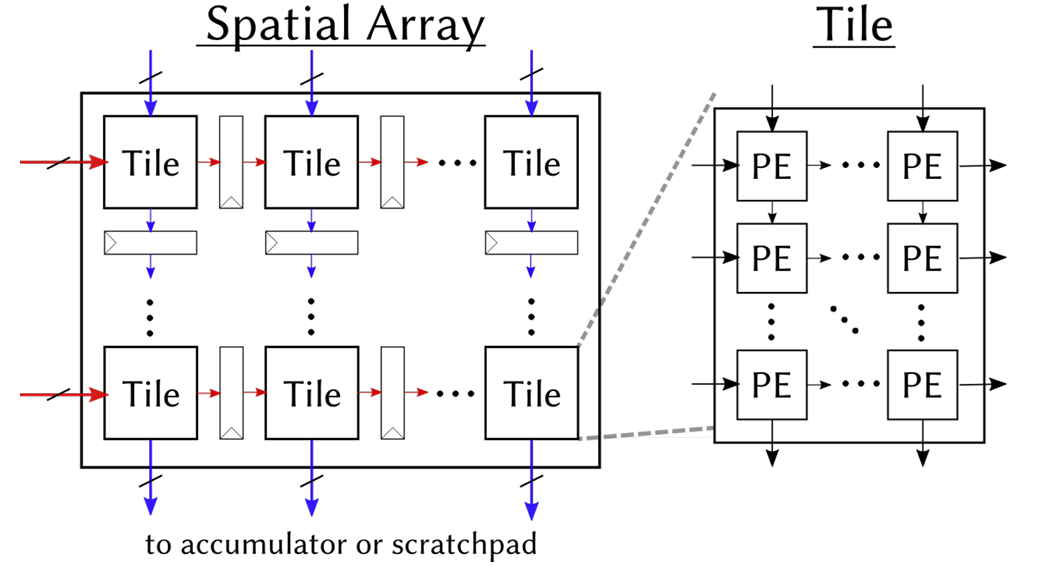
What each PE does internally is very simple:
c += a × b // one multiply-accumulate (MAC)
It receives a from the left and b from above, performs a multiply-accumulate with the existing partial sum c, then passes a to the PE on the right and b to the PE below. In our 8x8 configuration, the array has 64 PEs, and can simultaneously perform 64 Int8 multiply-accumulates every clock cycle.
2.2 Weight Stationary Mode
Systolic arrays have multiple dataflow modes that determine which data "stays" in the PEs and which data "flows" through the array. Our Gemmini configuration uses Weight Stationary (WS) mode -- weights are preloaded into the PEs and remain stationary, while input data and partial sums flow through the array.
Taking the computation C = A x B as an example (A is the input, B is the weights):
Step 1: Load weights. Distribute the elements of weight matrix B to each PE. PE(i,j) stores B[i][j]. Once loading is complete, the weights "reside" in the array and no longer move.
Step 2: Stream in inputs. Each row of input matrix A flows into the array from the left. Elements of row k of A enter the PEs in row k, advancing one column per clock cycle.
Step 3: Accumulate. Each PE performs one multiply-accumulate per cycle: it multiplies its stored weight by the incoming input value and adds the result to the partial sum. After K cycles (where K is the inner product dimension), the partial sum in each PE is the corresponding element of the output matrix C.
Step 4: Read out results. Read the completed output matrix from the bottom of the array (or from the accumulator).
The advantage of WS mode is that weights only need to be loaded once and can be reused many times. This is well-suited for inference scenarios -- the same set of model weights is used repeatedly with different inputs.
2.3 Tiling: Handling Matrices Larger Than the Array
An 8x8 array can only directly compute an 8x8 matrix multiplication. Real-world matrices are often much larger (e.g., 288x768), so what do we do?
The answer is tiling: slice the large matrix into many 8x8 blocks (tiles), feed them into the array one by one, and assemble the results at the end. For example, a 288x768 matrix multiplication is split into (288/8) x (768/8) = 36 x 96 = 3456 tiles for computation.
Gemmini's tiled_matmul_auto API handles tiling automatically -- you only need to pass in the matrix dimensions and pointers, and the tiling strategy is determined automatically by the hardware and runtime library. This is transparent to the application layer.
2.4 Local Storage: Scratchpad and Accumulator
Fetching data from main memory for every computation is too slow. Gemmini has two internal local storage areas to cache frequently accessed data:
- Scratchpad: Stores input matrix and weight data in int8 format. In our configuration: 32 KB (4 banks x 1024 rows x 8 bytes/row).
- Accumulator: Stores intermediate multiply-accumulate results (int32 partial sums). In our configuration: 16 KB (512 rows x 8 x 4 bytes/row).
The data flow is: Main memory -> DMA -> Scratchpad -> Systolic array -> Accumulator -> DMA -> Main memory. The DMA engine handles data transfers between main memory and local storage, and can be pipelined in parallel with computation.
3. Gemmini's Architecture Within Chipyard
3.1 The RoCC Interface
Gemmini connects to the Rocket Core through the RoCC (Rocket Custom Coprocessor) interface. The design philosophy of RoCC is straightforward: when the CPU encounters a custom instruction, it forwards the opcode and operands through a dedicated interface to an attached coprocessor, which executes the operation and writes the result back.
From the CPU's perspective, calling Gemmini is simply executing a custom instruction. This instruction is recognized by the Rocket Core's decoder as a RoCC instruction and forwarded to the Gemmini controller, triggering a series of operations including DMA transfers and systolic array computation. The CPU can continue executing subsequent instructions, or it can use a fence instruction to wait for Gemmini to finish.
On the software side, Gemmini provides a C header file (gemmini.h) that wraps RoCC instructions into C function calls. The most commonly used one is tiled_matmul_auto -- you pass in matrix dimensions, data pointers, and configuration parameters, and the underlying layer automatically handles tiling, DMA transfers, and array scheduling.
RoCC is not just Gemmini's interface -- it is the universal attachment mechanism for all custom accelerators in Chipyard. Once you've learned to walk through the "write Config -> synthesize Bitstream -> configure permissions -> invoke from user space" pathway with Gemmini, the process is exactly the same for other accelerators (e.g., a custom CNN accelerator, a cryptographic engine, or a signal processing unit). Only the accelerator's internal computation logic and software API change; the RoCC interface, permission configuration, and deployment process remain identical.
3.2 Full System Architecture
The figure below shows the complete architecture of the CPU and Gemmini connected via the RoCC interface. On the left is the Rocket Core (CPU), which sends instructions via RoCC Cmd and shares page tables via RoCC PTW. On the right is Gemmini's internal structure -- the Controller handles instruction parsing and dependency management, the DMA Engine transfers data between main memory and local storage, the Spatial Array (systolic array) performs matrix multiplication, and the Scratchpad and Accumulator provide on-chip caching.
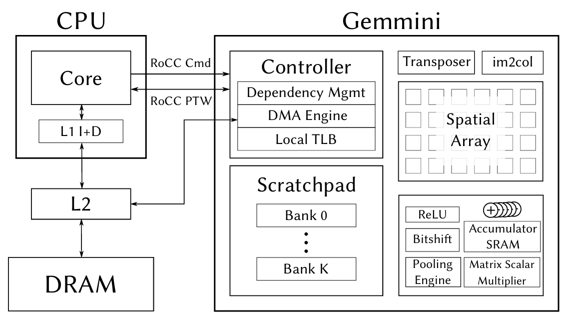
The figure also shows some Gemmini modules that we didn't use this time -- the Transposer (matrix transposition), im2col (convolution unrolling), Pooling Engine, etc. These are designed for CNN inference scenarios. We disabled them in the Config via has_training_convs = false and has_max_pool = false to save FPGA resources.
4. Hardware Configuration: Generating a Bitstream with Gemmini
4.1 Chipyard Config
The previous chapter used RocketNexysVideoFastUARTConfig, which only includes the Rocket Core. To add Gemmini, we need to write a new Config. The approach is to add two classes in fpga/src/main/scala/nexysvideo/Configs.scala:
The first is WithSmallGemmini, which defines Gemmini's hardware parameters:
class WithSmallGemmini extends Config((site, here, up) => {
  case BuildRoCC => up(BuildRoCC) ++ Seq(
    (p: Parameters) => {
      implicit val q = p
      val gemmini = LazyModule(new Gemmini(GemminiConfigs.defaultConfig.copy(
        meshRows = 8,                          // 8×8 array (default is 16×16)
        meshColumns = 8,
        sp_capacity = CapacityInKilobytes(32),  // Scratchpad 32KB
        acc_capacity = CapacityInKilobytes(16), // Accumulator 16KB
        has_training_convs = false,             // Disable training convolutions to save resources
        has_max_pool = false,                   // Disable pooling
        dataflow = Dataflow.WS,                 // Weight Stationary
        ld_queue_length = 4,                    // Reduced queue depth
        st_queue_length = 2,
        ex_queue_length = 4,
        acc_read_full_width = false,
        ex_read_from_acc = false,
        ex_write_to_spad = false
      )))
      gemmini
    }
  )
})
Why 8x8 instead of the default 16x16? Because the Artix-7 doesn't have enough BRAM. Gemmini's Scratchpad and Accumulator are entirely implemented using BRAM. A 16x16 array with the default 256 KB Scratchpad would require far more BRAM than the Nexys Video's 365 Block RAMs. Shrinking to 8x8 + 32 KB/16 KB brings BRAM utilization to roughly 96% -- just barely fitting.
The second is the top-level Config, which combines Gemmini, board-level configuration, and the Rocket Core:
class GemminiNexysVideoConfig extends Config(
  new WithSmallGemmini ++
  new WithNexysVideoTweaksFastUART ++
  new chipyard.config.WithBroadcastManager ++
  new chipyard.config.WithSystemBusWidth(128) ++ // Gemmini requires a 128-bit bus
  new chipyard.RocketConfig)
Note that WithSystemBusWidth(128) is required by Gemmini -- Gemmini's DMA needs a sufficiently wide bus to transfer data efficiently.
4.2 FPGA Resource Utilization
Post-synthesis resource utilization:
| Resource | Used | Available | Utilization |
|---|---|---|---|
| LUT | ~80,000 | 134,600 | 59% |
| FF | ~50,000 | 269,200 | 19% |
| BRAM | 350 | 365 | 96% |
| DSP | 48 | 740 | 6% |
BRAM is the only bottleneck -- nearly maxed out. LUT and FF have plenty of headroom, and DSP usage is minimal (Int8 multiplication doesn't require DSP slices). If your FPGA has more BRAM (e.g., the Virtex UltraScale+ on a VCU118), you can use a larger array and a bigger Scratchpad.
4.3 Synthesis and Programming
The process is the same as in the previous chapter, just with a different Config name:
cd ~/chipyard
source env.sh

# Generate Verilog (optional, for a quick sanity check of the configuration)
make -C fpga SUB_PROJECT=nexysvideo CONFIG=GemminiNexysVideoConfig verilog

# Synthesize Bitstream (requires Vivado, takes longer due to increased logic)
make -C fpga SUB_PROJECT=nexysvideo CONFIG=GemminiNexysVideoConfig bitstream
Synthesis takes considerably longer than with the bare Rocket Core (Gemmini adds a lot of logic) and may require one to two hours on a typical workstation. The programming step is exactly the same -- use Vivado Hardware Manager to flash the .bit file.
5. Software Prerequisites: Enabling User-Space Access to Gemmini
Gemmini is invoked via RoCC custom instructions. By default, RISC-V's privilege mechanism prohibits user-space programs from executing custom instructions -- this is for security. To allow user-space programs under Linux to call Gemmini, permissions need to be enabled at two levels.
5.1 OpenSBI: Setting mstatus.XS
The XS bits in the mstatus register control the state of custom extensions. If XS=0 (Off), any custom instruction will trigger an Illegal Instruction exception. We need to set XS to a nonzero value during OpenSBI initialization:
// lib/sbi/sbi_hart.c - mstatus_init()
mstatus_val |= MSTATUS_XS;  // Enable custom extensions
csr_write(CSR_MSTATUS, mstatus_val);
This step is done in M-mode, before the Linux kernel boots.
5.2 Linux Kernel: Enabling CONFIG_RISCV_ROCC
The Linux kernel needs to set sstatus.XS to Initial (01) when creating new processes, allowing user-space access to RoCC:
// arch/riscv/kernel/process.c - start_thread()
#ifdef CONFIG_RISCV_ROCC
    regs->status |= SR_XS_INITIAL;
#endif
Enable it in the kernel .config:
CONFIG_RISCV_ROCC=y
If either of these two steps is missing, user-space programs will receive SIGILL (Illegal Instruction) when executing Gemmini instructions. In dmesg, you can see that the badaddr corresponds to the RoCC instruction encoding.
6. Using Gemmini for Matrix Multiplication
6.1 Data Type: Int8
Our Gemmini configuration uses Int8 data types -- each PE in the systolic array performs int8 x int8 -> int32 multiply-accumulates. This means both the input matrix and the weight matrix must be in int8 format. If the original data is float32 (e.g., neural network weights), it needs to be quantized to int8 before being fed into Gemmini. The specific quantization scheme and implementation will be covered in detail in the next chapter alongside a real application.
This section focuses on how to call Gemmini -- assuming you already have int8 data, how to make Gemmini compute a matrix multiplication.
6.2 The tiled_matmul_auto API
Gemmini's core API is tiled_matmul_auto, defined in gemmini.h. This function takes matrix dimensions and pointers, and automatically handles tiling, DMA transfers, and systolic array scheduling:
tiled_matmul_auto(
    dim_I, dim_J, dim_K,    // Output I×J, inner product dimension K
    A, B,                    // Input matrices (int8)
    D, C,                    // Bias and output
    stride_A, stride_B, stride_D, stride_C,
    A_scale, B_scale, D_scale,
    activation,              // Activation function (NO_ACTIVATION / RELU)
    acc_scale,               // Accumulator scale factor
    bert_scale,
    repeating_bias,
    transpose_A, transpose_B,
    full_C, low_D,           // Output precision control
    weightA,
    WS                       // Dataflow mode: Weight Stationary
);
gemmini_fence();             // Wait for Gemmini to complete
There are many parameters, but most can be left at their defaults. The key ones are:
dim_I, dim_J, dim_K: Matrix dimensions, C(IxJ) = A(IxK) x B(KxJ)acc_scale: Scale factor from the int32 accumulator to the outputWS: Weight Stationary modegemmini_fence(): Called after issuing the compute instruction; the CPU waits for Gemmini to finish
6.3 A Simple Example
Suppose we want to compute C(d,1) = W(d,n) x x(n,1) -- a weight matrix multiplied by an input vector, the most common operation in neural network inference:
// W: d×n int8 weight matrix (already prepared)
// x: n×1 int8 input vector
// C: d×1 output

tiled_matmul_auto(
    d, 1, n,              // Output: d rows, 1 column; inner product dimension: n
    (elem_t*)W, x,        // Weights and input (both int8)
    NULL, C,              // No bias, output to C
    n, 1, 0, 1,           // Memory strides
    MVIN_SCALE_IDENTITY, MVIN_SCALE_IDENTITY, MVIN_SCALE_IDENTITY,
    NO_ACTIVATION,
    ACC_SCALE_IDENTITY,   // Accumulator scale factor
    0,
    false, false, false,
    false, false,         // full_C=false: output int8
    0, WS
);
gemmini_fence();
After this call, C contains the matrix multiplication result. From the programmer's perspective, the entire process is a single function call -- tiling, DMA, and array scheduling are all handled automatically.
6.4 A Real-World Pitfall: The full_C Parameter
tiled_matmul_auto has a full_C parameter that controls the output format:
full_C=true: Output int32 (preserving the full precision of the accumulator)full_C=false: Output int8 (the accumulator result is multiplied by acc_scale and truncated to int8)
We initially used full_C=true, and the output was all zeros. After investigation, we found that full_C=false is what works correctly with our hardware configuration. These subtle differences in API parameters are often not documented in detail -- you only discover them by actually running the code.
7. Verifying That Gemmini Works
Before deploying an LLM, use a simple test program to verify that the Gemmini hardware is functioning correctly. Gemmini provides a test suite (gemmini-rocc-tests) that can run on either the simulator or the FPGA.
7.1 Spike Simulation Verification
Spike is the RISC-V instruction set simulator and supports the Gemmini extension. Note that the default libgemmini uses DIM=16; you need a DIM=8 version matching your hardware configuration:
spike --extlib=/path/to/libgemmini_dim8/libgemmini.so \
      --extension=gemmini \
      pk ./gemmini_test_simple
The test program verifies two things: Scratchpad mvin/mvout data movement, and a 16x16 matrix multiplication via tiled_matmul_auto (larger than the array size, requiring tiling). Both tests pass, confirming that the Gemmini instructions and tiling logic are correct.
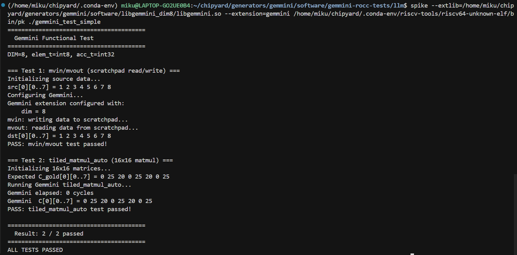
7.2 Verification on FPGA
Run the same test program on the FPGA to confirm that the hardware implementation behaves consistently with the simulation. The deployment path is essentially the same as in previous chapters -- compile the RISC-V program and load it onto the FPGA via UART-TSI.
Bare-metal programs can be loaded directly via uart_tsi. However, if you want to run test programs under Linux, there is one thing to keep in mind: after UART-TSI finishes loading fw_payload.elf, it becomes an interactive console and can no longer be used to transfer files. Therefore, programs and data files to be run under Linux need to be prepared in advance. There are two approaches:
- Bundle into initramfs: When building
fw_payload.elf, include the test programs in the root filesystem's cpio archive. The downside is that you need to recompile the kernel and firmware every time you change a file. - Use an SD card: Add an SPI peripheral in the Config (e.g.,
GemminiNexysVideoSDConfig), and mount the SD card in Linux to read files. Changing files only requires removing the card and copying to it -- no firmware rebuild needed.
The SD card approach is more convenient. It's tangential to the main topic, so feel free to explore it on your own. The companion repo's Configs.scala includes a ready-made GemminiNexysVideoSDConfig for reference.
Once verification passes, you can start building real applications on this foundation.
8. Summary
Let's recap what this chapter covered:
- Systolic array principles: PE array structure, Weight Stationary dataflow, tiling for large matrices
- Gemmini architecture: Connected to the Rocket Core via the RoCC interface, with built-in Scratchpad and Accumulator
- Hardware configuration: Writing a Chipyard Config with an 8x8 array + 32 KB/16 KB local storage, just barely fitting into the Artix-7
- Software permissions: Setting
mstatus.XSin OpenSBI, enablingCONFIG_RISCV_ROCCin Linux - Calling Gemmini: The
tiled_matmul_autoAPI -- just pass in matrix dimensions and int8 data
At this point, the hardware and software foundations are in place -- Gemmini can correctly execute matrix multiplication on the FPGA, and we understand how to use the API.
The Gemmini Config, OpenSBI patch, and Linux RoCC configuration discussed in this article are all in the companion repository:
GitHub: https://github.com/mikutyan4/chipyard-linux-nexys
Next chapter: Chapter 7 -- Running LLM Inference on FPGA with Gemmini. We'll apply Gemmini to real LLM inference -- how to quantize a float32 model to int8, how to deploy it to the FPGA, how much speedup the accelerator delivers in practice, and why a 75x improvement in matrix multiplication translates to only a 10x overall speedup.
Chapter 7: Running LLM Inference on FPGA with Gemmini
The previous chapter covered Gemmini's architecture and how to invoke it. This chapter puts it to real use — accelerating LLM inference on FPGA with Gemmini — and then uses profiling to observe the accelerator's actual impact.
The model used is the TinyStories 15M that ships with Andrej Karpathy's llama2.c — a scaled-down LLaMA 2 architecture with 6 Transformer layers and roughly 15 million parameters. Small as it is, the Transformer computation structure is complete, making it a clear window into how the accelerator performs under a real workload.
1. Overall Strategy: Which Operations Go to Gemmini
Not everything in a Transformer forward pass is matrix multiplication. Breaking it down layer by layer:
| Operation | Computation Type | Gemmini-Compatible |
|---|---|---|
| QKV Projection | Matrix multiplication | Yes |
| RoPE Positional Encoding | Trigonometric functions | No |
| Attention (QK^T + Softmax) | Sparse operations | No |
| Output Projection | Matrix multiplication | Yes |
| RMSNorm | Element-wise operations | No |
| FFN (W1, W3) | Matrix multiplication | Yes |
| SiLU Activation | Element-wise nonlinearity | No |
| FFN (W2) | Matrix multiplication | Yes |
| Classifier | Matrix multiplication | Yes |
Each layer has 7 matrix multiplications (wq, wk, wv, wo, w1, w2, w3), plus the final Classifier — all of these go to Gemmini. The remaining operations — RMSNorm, RoPE, Attention, SiLU, etc. — stay on the CPU and run in float32.
2. Int8 Quantization
2.1 Why Quantize
As mentioned in the previous chapter, our Gemmini is configured for the Int8 data type — the PEs perform int8 × int8 → int32. But the model weights are float32, so they must be quantized before Gemmini can process them.
The core idea of quantization is mapping the continuous float32 values to the 256 discrete values of int8 (-128 to 127). The mapping strategy determines how much precision is lost.
2.2 Approach: Per-Tensor Symmetric Quantization
We use the simplest approach — per-tensor symmetric quantization:
scale = max(|tensor|) / 127
quantized = round(tensor / scale)
Take the maximum absolute value across the entire tensor and linearly map it to ±127. Each tensor requires only a single scale value.
2.3 Weight Quantization (Offline)
Weights are fixed before inference, so we quantize them ahead of time with a Python script:
def quantize_tensor(tensor):
    scale = np.max(np.abs(tensor)) / 127
    quantized = np.round(tensor / scale).clip(-128, 127).astype(np.int8)
    return quantized, scale
For each layer, the 7 weight matrices get their own scale and are converted to int8. Token embedding and RMSNorm weights remain in float32 (they are not involved in matrix multiplications).
2.4 Activation Quantization (Static Calibration)
Activations are produced dynamically during inference. We run a float32 inference pass over 5 sample sequences, record the maximum absolute value at each activation point in every layer, and multiply by a 1.2x margin to obtain the scale:
calibration_tokens = [
    [1, 450, 2501, 263, 931],   # "Once upon a time"
    [1, 13, 851, 338, 263],     # "There was a"
    ...
]
This way, all scales are known constants at inference time — no runtime dynamic computation is needed.
2.5 Verification
After quantization, we first verify on x86:
./llama2_int8_x86 stories15M_int8.bin -n 64 -i "Once upon a time"
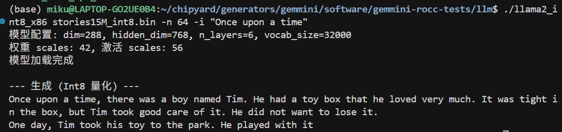
(The prompt messages in the screenshot are in Chinese; the version in the companion repo has been translated to English.)
The output on x86 is largely coherent, but a careful look reveals occasional unnatural expressions — this is the precision loss from int8 quantization. The per-tensor symmetric quantization we use is the simplest scheme: the entire tensor shares one scale, and if the weight distribution is uneven (some channels have a large range while others are tiny), many small values get quantized to 0, losing information. On the FPGA there is an additional int32→int8 intermediate truncation step, causing errors to accumulate further.
Common improvements used in industry include: per-channel quantization (computing a separate scale for each output channel, significantly improving precision), SmoothQuant (rebalancing the quantization difficulty between weights and activations through mathematically equivalent transformations), and GPTQ/AWQ (weight optimization methods that minimize quantization error using calibration data). The core idea behind all of these techniques is to make more precise use of int8's 256 discrete values to approximate the original float32 distribution. Interested readers can start with the SmoothQuant paper — the intuition is very straightforward.
Quantization precision optimization is an independent research direction in its own right and falls outside the scope of this tutorial. Here we use the simplest scheme to get the pipeline working end-to-end, and focus on the profiling and accelerator analysis that follow.
3. Gemmini-Accelerated matmul
With int8 data in hand, we can call Gemmini. The full matrix multiplication flow is:
void matmul_gemmini(float* xout, float* x, int8_t* w,
                    float w_scale, float x_scale, float out_scale,
                    int n, int d) {
    // 1. Quantize input: float32 → int8
    for (int i = 0; i < n; i++) {
        int32_t q = (int32_t)roundf(x[i] / x_scale);
        g_B[i] = clamp(q, -128, 127);
    }

    // 2. Compute acc_scale: controls scaling from int32 accumulator to int8 output
    float acc_scale = (w_scale * x_scale) / out_scale;

    // 3. Gemmini computation: C(d,1) = W(d,n) × x(n,1)
    tiled_matmul_auto(
        d, 1, n,
        (elem_t*)w, g_B,
        NULL, g_C,
        n, 1, 0, 1,
        MVIN_SCALE_IDENTITY, MVIN_SCALE_IDENTITY, MVIN_SCALE_IDENTITY,
        NO_ACTIVATION, acc_scale, 0,
        false, false, false,
        false, false,    // full_C=false: output int8
        0, WS
    );
    gemmini_fence();

    // 4. Dequantize output: int8 → float32
    for (int i = 0; i < d; i++) {
        xout[i] = (float)((int8_t)g_C[i]) * out_scale;
    }
}
CPU quantizes the input → Gemmini performs the int8 matrix multiplication → CPU dequantizes the output. The matrix multiplication itself is done in hardware; the CPU is only responsible for data format conversion on both ends.
4. Deploying to the FPGA
4.1 Compiling the LLM Program
Cross-compile with Chipyard's RISC-V toolchain, statically linked:
source ~/chipyard/env.sh
cd gemmini-llm
make CHIPYARD=~/chipyard llm llc
llm is the Gemmini-accelerated version; llc is the CPU-only version (used as a baseline). Both include profiling timers.
4.2 Packing initramfs
After Linux boots, UART-TSI becomes the interactive console and can no longer be used to transfer files. The LLM program and model must be packed into initramfs ahead of time:
cd /tmp && mkdir -p initramfs_llm && cd initramfs_llm

fakeroot sh -c "
  cpio -idm < ~/chipyard/software/firemarshal/images/prototype/br-base/initramfs.cpio 2>/dev/null
  mkdir -p root/llm
  cp /path/to/llm root/llm/
  cp /path/to/llc root/llm/
  cp /path/to/stories15M_int8_v2.bin root/llm/m2.bin
  cp /path/to/tokenizer.bin root/llm/t.bin
  chmod 755 root/llm/llm root/llm/llc
  chown -R root:root .
  find . | cpio -o -H newc > ~/initramfs_llm.cpio
"
Key point: you must use fakeroot to ensure file ownership is root:root, otherwise the kernel will Kernel Panic when parsing the cpio archive.
After packing, update the kernel's CONFIG_INITRAMFS_SOURCE, then recompile Linux and OpenSBI to generate a new fw_payload.elf.
Alternatively, you can use the SD card approach (GemminiNexysVideoSDConfig) — place the files on an SD card, mount and read them after Linux boots, and avoid recompiling the firmware each time.
4.3 Flashing and Booting
- Flash the
GemminiNexysVideoConfigbitstream with Vivado - Load
fw_payload.elfviauart_tsi_interactive(921600 baud, ~12 minutes because the LLM model is included) - Log in to Linux (root / fpga)
5. Results
After logging in, navigate to the /root/llm directory. First, run the CPU version as a baseline:
./llc m2.bin -z t.bin -n 8 -t 0 -i "Once upon a time"
Then run the Gemmini-accelerated version:
./llm m2.bin -z t.bin -n 8 -t 0 -i "Once upon a time"
Both versions produce English stories. -t 0 selects greedy mode (always pick the highest-probability token), yielding deterministic output for easier comparison.
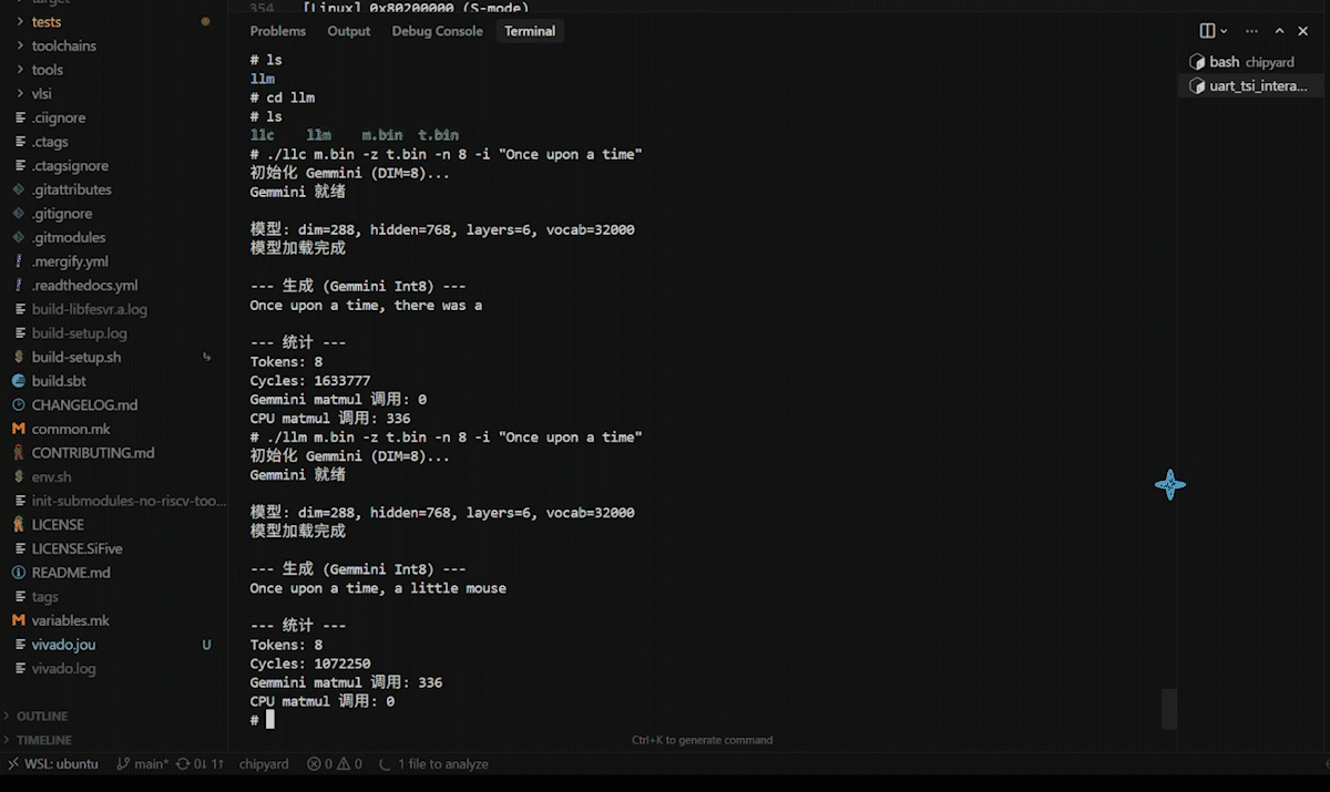
6. Profiling-Driven Optimization
This section is the heart of the chapter — not a one-shot result, but an iterative cycle of profiling → identifying the bottleneck → targeted optimization → profiling again.
6.1 Round 1: Accelerating matmul, but Only a 1.52x Speedup
After replacing all QKV and FFN matrix multiplications with Gemmini calls, we ran the comparison test with high expectations:
| Version | Cycles (8 tokens) | Speedup |
|---|---|---|
| CPU int8 | 1,633,777 | 1.00x |
| Gemmini int8 | 1,072,250 | 1.52x |
Only 1.52x? Gemmini should be much faster on matrix multiplications. Where is the problem?
Without profiling, you cannot know.
6.2 Adding Profiling, Finding the Real Bottleneck
We inserted rdtime timing calls before and after each key operation, recompiled, and ran again. Profiling results:
--- Profiling (8 tokens) ---
Total cycles:          1,056,147

Classifier (CPU)         913,481   89.49%   ← !!
Sampling                  58,982    5.78%
Softmax                   14,566    1.43%
Other                     69,118    3.30%
The Classifier consumed 89.5% of the time.
The reason: the Classifier is a vocab_size(32000) × dim(288) matrix multiplication — a massive computation (18.4 million float operations). But it uses the token embedding weights, which had been kept in float32 without quantization, so it did not go through Gemmini and was computed on the CPU in float32.
All the other matrix multiplications (QKV, FFN, etc.) were already accelerated by Gemmini and ran fast. But the Classifier alone ate 89.5% of the total time.
6.3 Round 2: Handing the Classifier to Gemmini Too
The fix: quantize the token embedding to int8 as well and switch the Classifier to use Gemmini.
Specific changes:
quantize.py— add int8 quantization for the embedding and generate a new model filellama2_int8_gemmini.c— change the Classifier to usematmul_gemmini
We first verified the quantized Classifier's precision on x86: logits correlation 0.997, top-5 tokens identical.
6.4 After Optimization: 10x Speedup
Profiling results after optimization:
| Metric | Before | After | Improvement |
|---|---|---|---|
| Total cycles | 1,056,147 | 163,474 | 6.5x |
| Classifier | 913,481 (89.5%) | 5,192 (5.3%) | 176x |
| Cycles/token | 132,018 | 20,434 | 6.5x |
Compared with the CPU baseline:
| Version | Cycles (8 tokens) | Speedup |
|---|---|---|
| CPU int8 | 1,633,777 | 1.00x |
| Gemmini (initial) | 1,072,250 | 1.52x |
| Gemmini (optimized) | 163,474 | 10.0x |
Speedup on the matrix multiplication portion alone: 75x.
Final throughput: ~3 tok/s in greedy mode, ~2 tok/s in top-p mode.
6.5 The New Bottleneck After Optimization
With the Classifier no longer the bottleneck, the time distribution shifted to:
| Phase | Share | Description |
|---|---|---|
| forward() computation | 52% | Attention + SiLU + RoPE and other CPU operations |
| I/O (serial output) | 40% | Hardware limitation of 921600 baud |
| Sampling | 8% | top-p sorting |
The new bottleneck is no longer matrix multiplication, but CPU-side Attention computation, activation functions, and serial I/O. None of these can be accelerated by Gemmini.
7. Why 75x matmul Speedup Yields Only 10x Overall Speedup
This is a vivid illustration of Amdahl's Law.
If the original matrix multiplication accounts for p% of total time and is sped up by a factor of S, then the overall speedup is:
Overall speedup = 1 / ((1 - p) + p/S)
In our case, matrix multiplication accounts for roughly 87% (after optimizing the Classifier), and S = 75:
1 / ((1 - 0.87) + 0.87/75) = 1 / (0.13 + 0.012) = 7.0x
This is broadly consistent with the measured ~10x (the difference comes from cache effects and overhead variations).
Key takeaway: An accelerator can only speed up the portion it handles. Even with a 75x speedup on matrix multiplications, the remaining 13% of CPU operations sets the ceiling for overall speedup at roughly 7-8x. To push further, operations like Attention and SiLU would also need to be offloaded to hardware — which is exactly the design philosophy behind industrial AI accelerators (GPUs, TPUs, NPUs).
8. Performance Comparison and Discussion
8.1 Comparison with Other Platforms
| Platform | Model | Speed | Power |
|---|---|---|---|
| This experiment (FPGA) | 15M | ~3 tok/s | ~5W |
| Raspberry Pi 4 | 15M | ~10 tok/s | ~5W |
| Apple M1 | 7B | ~10 tok/s | ~15W |
| RTX 3080 | 7B | ~50 tok/s | ~300W |
In absolute performance the FPGA is not competitive — a 50MHz Rocket Core with an 8×8 systolic array simply cannot match mature CPUs/GPUs in raw compute. But that is not the point.
8.2 The Value of This Demo
The value of this experiment lies not in the performance numbers themselves, but in demonstrating the complete closed loop from hardware accelerator design to application deployment:
- Hardware layer: Configure systolic array parameters in Chisel, synthesize to FPGA
- System layer: OpenSBI and Linux kernel configuration for RoCC permissions
- Algorithm layer: Int8 quantization scheme, precision-performance tradeoff
- Application layer: Integrate quantization and Gemmini calls into LLM inference
- Analysis layer: Profiling to locate bottlenecks, iterative optimization
This pipeline happens every day in industrial AI chip projects — just at a larger scale, with wider arrays, higher frequencies, and more complex software stacks. But the fundamental methodology is the same: hardware provides compute, software manages data flow, and profiling guides optimization.
8.3 Utilization Issues with the 8×8 Array
Current LLM inference generates one token at a time (Batch=1), so each matrix multiplication is a vector-matrix multiply (1×n @ n×d). Only 1 of the 8 rows in the 8×8 array is active, yielding a utilization of just 12.5%.
Ways to improve utilization:
- Prefill phase: When processing a long prompt, multiple tokens can be batched together
- Larger models: Larger matrix dimensions allow more effective tiling
- Batched inference: Processing multiple requests simultaneously
9. Summary
What this chapter accomplished:
- Quantization: Per-tensor symmetric int8 quantization with offline weight quantization + static activation calibration
- Modifying llama2.c: Connected 7 matrix multiplication layers + the Classifier to Gemmini
- Deployment: initramfs packing, fw_payload.elf compilation, FPGA loading
- Profiling-driven optimization: Discovered the Classifier was a 89.5% bottleneck → quantized the embedding → achieved 10x overall speedup
- Analysis: Amdahl's Law explains why a 75x matmul speedup translates to only a 10x overall speedup
Profiling is a prerequisite for optimization — without measurement you cannot know where the bottleneck lies. Once the first bottleneck is resolved, the next one surfaces. This iterative process itself is the most important methodology in performance optimization.
Additionally, while this chapter uses an LLM as the demonstration, the same path applies to other models. If you want to run YOLO object detection, Diffusion-based image generation, or any other model that involves matrix multiplications, the workflow is the same: quantize model weights to int8, implement forward inference in C, hand off matrix multiplications to Gemmini via tiled_matmul_auto, and leave the remaining operations on the CPU. The only difference is model structure — convolutions can be unrolled into matrix multiplications (im2col), and the U-Net in Diffusion models is also full of matmuls. The core quantization, invocation, deployment, and profiling pipeline can be reused directly.
We recommend actively using AI coding tools such as Copilot, Claude Code, and Cursor for this kind of engineering work. Questions like "should Gemmini's full_C parameter be true or false" or "what to do when int8 quantization precision is insufficient" are extremely tedious to track down manually in tens of thousands of lines of code, but pasting the symptoms and code snippets into an AI assistant can help you narrow down the problem quickly.
The quantization scripts, LLM inference code, and Makefiles discussed in this chapter are all available in the companion repo:
GitHub: https://github.com/mikutyan4/chipyard-linux-nexys
This is the final main chapter of the series. By reaching this point, you now have a configurable processor core, a customizable hardware accelerator, a complete Linux software stack running on an FPGA, and end-to-end experience deploying AI models on it and analyzing performance with profiling. As a researcher in the AI chip space, this essentially covers the foundational skills for research in the field — from here, whether you pursue accelerator microarchitecture optimization, quantization algorithm improvements, or dataflow design space exploration, you can work directly on this platform.
Some thoughts this series aims to convey — about reuse and about AI tools — are saved for the conclusion: Conclusion — Standing on the Shoulders of Giants to Do Computer Architecture Research.
Conclusion: Doing Architecture Research on the Shoulders of Giants
We've reached the end. The entire series is now complete.
From setting up the environment, running simulations, and understanding the tapeout process, to booting Linux on an FPGA, and then integrating the Gemmini systolic array to run LLM inference -- you now have a complete system spanning hardware, operating system, and accelerator applications. If you followed along step by step, this journey was certainly not easy: all kinds of errors, unfamiliar concepts, debugging across multiple abstraction layers. But you made it through. Congratulations.
I. Our Methodology
Looking back, what this entire series did can be summed up in one sentence: assemble existing components, then focus on the things we actually care about.
We used Rocket Core for the CPU, Linux for the operating system, Gemmini for the accelerator, and GCC for the compiler -- we didn't write any of them ourselves. What we did was configure them, wire them together, get them running on real hardware, and then run applications, do profiling, and optimize on top of that foundation.
The payoff of this approach is straightforward: in roughly one to two weeks, we completed the entire pipeline from environment setup to running LLM-accelerated inference on an FPGA -- including the ability to export tapeout-grade RTL design files.
I used to lean toward building everything from scratch myself. Then, while working on projects, I realized that things I spent ages implementing were often just a git clone away in the open-source community. After shifting my mindset, my productivity improved dramatically. This series is also meant to share that lesson -- you don't have to reinvent the wheel. Optimizing and exploring on top of an already mature system can yield equally deep understanding, and it drives you to read more cutting-edge papers and explore broader resources, actually widening your perspective.
The same philosophy applies to AI tools. Honestly, without AI assistance, it would have been very difficult for me to navigate the entirety of Chipyard on my own. The getchar return value validation bug in OpenSBI, the hvc0 console configuration in the Linux kernel, the full_C parameter behavior in Gemmini -- these issues span multiple repositories and tens of thousands of lines of code. Debugging them manually is extremely inefficient, but describing the symptoms to AI lets you narrow down the scope quickly.
A tool is just a tool. Using AI is no fundamentally different from using an IDE or a search engine. What matters is the problem you solved, not the tool you used to solve it. If you haven't yet deeply used AI programming tools like Copilot, Claude Code, or Cursor, I'd recommend giving them a try -- especially for cross-layer system debugging scenarios like this one.
II. What This Series Covered -- and What It Didn't
What we covered:
- Chipyard environment setup and toolchain
- Rocket Core simulation and HelloWorld
- Chipyard's role in the chip design flow
- Complete theory and practice of booting Linux on FPGA
- Gemmini systolic array principles and hardware configuration
- Accelerating LLM inference with Gemmini + profiling analysis
What we didn't cover, but you can follow the same patterns for:
- BOOM (out-of-order superscalar processor): used exactly the same way as Rocket -- just swap the Config
- Other accelerators: same RoCC deployment path as Gemmini -- write a Config, synthesize, set permissions, invoke
- Other models and applications: just write (or find) the source files, cross-compile, and package them into initramfs or an SD card
- Tapeout backend: Chipyard can export RTL, but the backend flow from RTL to GDS (synthesis, place-and-route, timing closure) is a separate topic entirely
At its core, what this series built is a framework. When you want to dive deeper into any particular part -- whether it's optimizing CPU microarchitecture, designing a new accelerator, or improving quantization algorithms -- you'll need domain-specific knowledge for that area, but the rest of the system can be reused directly without building from scratch.
III. Why I Wrote This Series
Chipyard is an excellent open-source architecture research platform, continuously maintained by the Berkeley team for many years. But I noticed there was never a sufficiently complete end-to-end tutorial -- one that could take you all the way from environment setup to running accelerator applications on an FPGA. Scattered posts exist, but stitching together the entire pipeline involves a tremendous number of pitfalls.
The original motivation for this series was to fill that gap: to create content that couldn't easily be found elsewhere, but that would genuinely help people.
Halfway through writing, I actually hesitated, thinking maybe no one would read it and my time was already tight. It was feedback and encouragement from readers that kept me going until the content was complete. Thank you all.
IV. Final Words
If you followed this series all the way through, what you now have is a complete architecture experimentation platform -- a configurable processor core, a customizable accelerator, Linux running on a real FPGA, and a verified software stack. Many researchers in computer architecture spend a long time building up a similar environment.
What you do next depends on your own research direction. Here are a few active and potentially fruitful areas on this platform: design space exploration of accelerator dataflows (WS/OS/hybrid), hardware-software co-designed quantization strategies (e.g., hardware-aware mixed-precision), scratchpad and DMA scheduling optimization, and end-to-end verification of custom RoCC accelerators. All of these can be pursued directly on the system we've built, without setting up the environment from scratch.
If you've hit new pitfalls during reproduction, adapted to a new FPGA board, or gotten a new model or application running, feel free to open an Issue or PR on the GitHub repo. Many people encounter problems but few share their solutions -- a single tip from you could save someone else an entire day of debugging.
Best of luck.
Companion code: https://github.com/mikutyan4/chipyard-linux-nexys